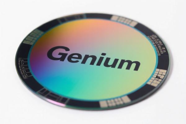
Gallium Nitride Wafer
CN → US| HS编码 | 关税税率 | 原产国 | 目的国 | 文档 |
|---|---|---|---|---|
| 3818000095 | 60.0% | CN | US | 官方文档 |
| 3818000010 | 60.0% | CN | US | 官方文档 |
| 8541590040 | 10.0% | CN | US | 官方文档 |
| 8541491010 | 60.0% | CN | US | 官方文档 |
| 3824991100 | 35.0% | CN | US | 官方文档 |
| 3824991100 | 35.0% | CN | US | 官方文档 |
商品图片
AI分析
💎 Gallium Nitride (GaN) Wafers: High-Voltage Semiconductors & The 50% Tariff Trap
🌐 HS Code Reference & Customs Clearance Guide | 2026 Latest Tariff Analysis | Professional Clearance Strategy
📌 I. Product Definition & Classification: Are You Shipping Raw Material or a Component?
Gallium Nitride (GaN) is a wide-bandgap semiconductor material revolutionizing power electronics (EV chargers, 5G infrastructure, fast chargers). In international trade, the classification depends strictly on the form and doping status of the wafer.
Key Distinction:
- Doped Wafers (3818): Crystals cut into wafers/dics specifically for electronics. This is the most common classification for raw GaN substrates ready for chip fabrication.
- Unmounted Chips/Dice (8541): If the wafer has already been processed into individual dies/chips but not packaged.
⚠️ Critical Warning:
- Do NOT classify GaN wafers as "Electronic Components" (Chapter 85) if they are still raw wafers/substrates. They must go to Chapter 38.
- Confusion often arises between3818.00.00.10(Gallium Arsenide) and3818.00.00.95(Other). GaN is "Other" because it is not Gallium Arsenide.
📦 II. HS Code Classification Details (2026 Latest Tariff Authority Comparison)
| HS Code | Product Description | Applicable Scenario | Doping Status |
|---|---|---|---|
3818.00.00.95 |
Chemical elements doped for use in electronics, in the form of discs, wafers or similar forms; chemical compounds doped for use in electronics Other | GaN Wafers, SiC Wafers, or other compound semiconductor substrates (not Gallium Arsenide). | ✅ Doped/Processed for Electronics |
3818.00.00.10 |
Chemical elements doped for use in electronics... Gallium arsenide wafers, doped | Strictly for GaAs (Gallium Arsenide). Do NOT use for GaN. | ✅ Doped GaAs Only |
8541.59.00.40 |
Other semiconductor devices... Unmounted chips, dice and wafers | Only if the "wafer" is actually a processed chip/die ready for packaging, not a raw substrate. | ✅ Processed into Device |
8541.49.10.10 |
Other diodes... Unmounted chips, dice and wafers | If the wafer consists of finished diode structures (not just substrate). | ✅ Finished Diode Structure |
🔍 Key Reminder:
- Most raw GaN Wafers (substrates for epitaxy) fall under3818.00.00.95.
- Gallium Arsenide (GaAs) has a specific subheading (3818.00.00.10). GaN does NOT. This is a common customs error.
- If the product is a finished chip (not a wafer), use Chapter 85 (8541...). If it is a wafer/substrate, use Chapter 38 (3818...).
💰 III. 2026 Latest Tariff Rate Breakdown (Including Surtaxes & Policy Add-ons)
✅ Applicable Country: United States (US)
✅ Origin: China (CN)
✅ Effective Time: November 10, 2025 onwards (including subsequent imports)
🎯 1. 3818.00.00.95 —— Gallium Nitride (GaN) Wafers / Other Doped Electronic Materials
| Item | Content |
|---|---|
| Base Tariff | 0.0% |
| USITC Surtax | +50.0% (Section 301 Tariff) |
| IEEPA Surtax | 0.0% (Not applicable for this specific code under current IEEPA lists provided in DATA) |
| Total Tax Rate | 50.0% |
| Tax Calculation | CIF Value × 50% |
| De Minimis Eligibility | ❌ NO (deny_de_minimis) |
| Legal Basis Path | USITC:3818.00.00.95 → SECTION_301:TARIF_50% |
📌 Explanation:
- GaN wafers are classified as "Other" doped electronic materials.
- They are subject to the full 50% Section 301 additional duty.
- There is NO base tariff (0%), so the 50% is the total impact.
- This is a HIGH tariff category. Cost planning must include this 50% surcharge.
🎯 2. 3818.00.00.10 —— Gallium Arsenide Wafers (For Comparison Only)
| Item | Content |
|---|---|
| Base Tariff | 0.0% |
| USITC Surtax | +50.0% |
| Total Tax Rate | 50.0% |
| De Minimis Eligibility | ❌ NO |
📌 Note:
- Although GaAs has a specific code, the tax rate is identical to "Other" (3818.00.00.95).
- Crucial: Using3818.00.00.10for GaN is a misclassification error, even if the tax rate is the same. It can lead to audits or penalties.
🛠️ IV. Customs Clearance Practical Advice (Real-World Pitfall Guide)
✅ 1. Required Documentation Checklist (Non-negotiable)
| Document | Must Provide | Explanation |
|---|---|---|
| ✅ Product Specification Sheet | ✔️ | Must state: Material (GaN), Form (Wafer/Disc), Diameter, Thickness, Doping Type (N/P-type). |
| ✅ Technical Data Sheet | ✔️ | Prove it is a "doped chemical compound/element for electronics." |
| ✅ Commercial Invoice | ✔️ | Description: "Gallium Nitride Semiconductor Wafer, Doped, for Electronic Use." Do NOT write "GaN Chip" if it's a wafer. |
| ✅ Certificate of Origin (CO) | ✔️ | To confirm Chinese origin (triggers the 50%). |
| ✅ HS Code Pre-classification Ruling | ✔️ | Highly recommended for high-value semiconductor imports to avoid disputes. |
✅ 2. Declaration Tips (Key Mantra)
🔥 “Wafer is Material (3818), Chip is Device (8541). GaN is 'Other', not GaAs!”
| Scenario | Correct Declaration | Error | Consequence |
|---|---|---|---|
| Raw GaN Wafer (Substrate) | 3818.00.00.95 |
3818.00.00.10 (GaAs) |
Misclassification risk; audit flag. |
| Raw GaN Wafer (Substrate) | 3818.00.00.95 |
8541.59.00.40 (Chip) |
Wrong chapter; potential delay. |
| Processed GaN Die/Chip | 8541.59.00.40 |
3818.00.00.95 |
Wrong chapter; may under/overpay duties depending on specific chip type. |
| Packaging Material | 3818.00.00.95 (if included) |
Separate line item | Ensure principal product is declared first. |
✅ 3. Special Handling Cases
| Scenario | Handling Advice |
|---|---|
| GaN on Si (Gallium Nitride on Silicon) | Still classified under 3818.00.00.95 as a "chemical compound doped for use in electronics." |
| Epi-Wafer (Epitaxial Layer) | If heavily processed into a device structure, may move to 8541. Consult a customs broker for borderline cases. |
| High-Value Single Wafer | Ensure accurate CIF valuation. The 50% tax applies to the entire value. |
| Sample vs. Commercial | Both are subject to 50%. No de minimis exemption. |
🌍 V. Global Market Comparison (2026 Latest)
| Country/Region | Recommended HS Code | Tariff | Certification | Notes |
|---|---|---|---|---|
| 🇺🇸 USA | 3818.00.00.95 |
50% (China Origin) | None specific, but 301 applies | High Cost. Plan accordingly. |
| 🇨🇳 China | 3818.00.00.95 |
0-6% (depending on trade agreement) | N/A | No 301 tax. |
| 🇪🇺 EU | 3818.00.99 |
0-5% (Standard MFN) | CE/RoHS | No punitive tariffs. |
| 🇬🇧 UK | 3818.00.99 |
0-5% | UKCA | Post-Brexit rules apply. |
| 🇯🇵 Japan | 3818.00.90 |
0-5% | PSE | Liberal trade. |
📌 Conclusion:
- USA is the only major market imposing a 50% punitive tariff on GaN wafers from China.
- Supply chain diversification (e.g., sourcing from US/EU/JP) can avoid this cost, but at the expense of raw material cost.
- Domestic processing in China and exporting finished chips (also 50%+) remains challenging but is the current industry norm.
📌 VI. Common Mistakes & Pitfall Guide (Lessons Learned)
❌ Mistake 1: Classifying GaN Wafer as 3818.00.00.10 (Gallium Arsenide)
👉 Consequence: Even though the rate is the same (50%), it is a false declaration. Customs may seize goods or issue penalties for incorrect HS code usage.
Correct: Use 3818.00.00.95 ("Other").
❌ Mistake 2: Declaring as 8541 (Semiconductor Devices) when it is a raw wafer
👉 Consequence: May be delayed for "insufficient information." The 50% tax is the same, but the regulatory oversight is higher for Chapter 85 (may require additional security checks).
Correct: Use 3818 for raw/doped wafers.
❌ Mistake 3: Ignoring the 50% Surtax in cost calculation
👉 Consequence: Margin erosion. 50% is half the value!
Correct: Include 50% in all Landed Cost models.
❌ Mistake 4: Using "De Minimis" for small samples
👉 Consequence: Denied. Semiconductor materials are explicitly excluded from de minimis exemptions under Section 301.
Correct: Pay duties on ALL shipments.
✅ Correct Practice:
“Gallium Nitride (GaN) Semiconductor Wafer, Doped, 4-Inch, N-Type, for Electronic Device Fabrication, HS 3818.00.00.95, Origin: China”
🎯 VII. Conclusion: Precision Classification Saves Money & Time
🎯 Remember the Mantra:
🔹 “GaN is NOT GaAs (Use 95, not 10).”
🔹 “Wafer is Material (3818), Chip is Device (8541).”
🔹 “50% Tax is Real, No De Minimis, Pay Up!”
📌 Pro Tip:
If your GaN wafers are not from China (e.g., from the US, Europe, or Southeast Asia), the 50% Section 301 tariff DOES NOT APPLY.
✅ Action:
📞 Verify Origin on your CO.
📋 Request Pre-Ruling from CBP for borderline cases (Wafer vs. Chip).
📊 Calculate Landed Cost including 50% if CN Origin.
📣 Immediate Action:
🛑 STOP if you are using
3818.00.00.10for GaN.
✅ UPDATE your customs broker to use3818.00.00.95.
💼 Budget for the 50% duty to protect your profit margins.
✨ Professional Clearance Starts with Accurate Classification!
💼 Your Wafer’s Value is High, Don’t Let Tariffs Destroy Your Margin!
用户评价
关于 HS 编码归类
协调制度(HS)是由世界海关组织(WCO)制定的国际贸易商品分类标准。全球 200 多个国家采用 HS 系统作为海关关税、贸易统计和进出口监管的基础。
每个 HS 编码遵循以下层级结构:
- 章(2 位)——商品大类(例如:第 84 章:机器和机械设备)
- 品目(4 位)——章内的更具体分类
- 子目(6 位)——国际通用细分,所有 WCO 成员国统一使用
- 本国细分(8-10 位)——各国自行扩展的细分编码,如美国 HTSUS 10 位编码
正确的 HS 编码归类对于顺利通关、准确缴纳关税和遵守贸易法规至关重要。错误归类可能导致海关延误、多缴关税或罚款。
从CN进口到US时,适用的关税税率可能包括:
- 最惠国(MFN)税率——适用于 WTO 成员国的标准关税税率
- 普通税率——适用于无贸易协定国家
- 贸易救济关税——附加关税,如 301 条款(反倾销)、232 条款(国家安全)或反补贴税
本页内容仅供参考。如需正式归类,请咨询当地海关或持牌报关代理。