P type Doped Silicon Wafer
CN → US| HS编码 | 关税税率 | 原产国 | 目的国 | 文档 |
|---|---|---|---|---|
| 3818000020 | 60.0% | CN | US | 官方文档 |
| 2804691000 | 15.3% | CN | US | 官方文档 |
| 2804695000 | 15.5% | CN | US | 官方文档 |
| 3824991100 | 35.0% | CN | US | 官方文档 |
| 3824991900 | 41.5% | CN | US | 官方文档 |
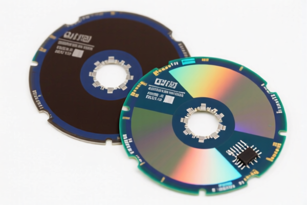
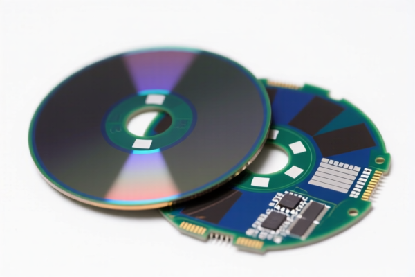
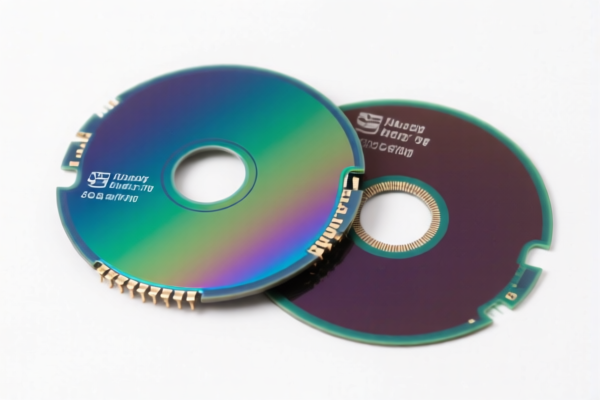
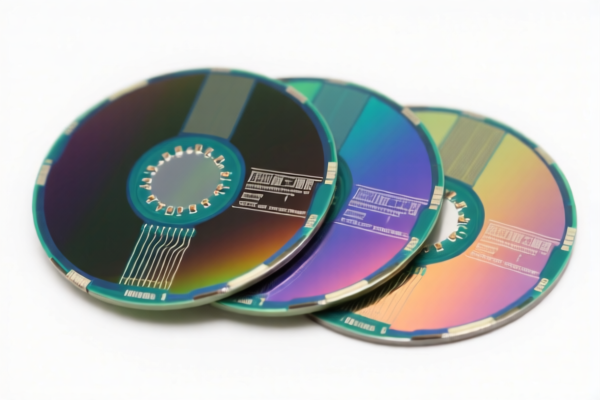
商品图片
AI分析
💎 P-Type Doped Silicon Wafer (Semiconductor Substrates)
🌐 HS Code Reference & Customs Clearance Guide | 2026 Latest Tariff Analysis | Professional Strategy for Silicon Wafers
📌 1. Product Definition & Classification: What Exactly is a "P-Type Doped Silicon Wafer"?
A P-Type Doped Silicon Wafer is a foundational material in the semiconductor industry, serving as the substrate for integrated circuits, power electronics, and sensors. Unlike raw silicon, these wafers have undergone specific doping processes (typically with Boron) to modify their electrical properties, making them suitable for semiconductor manufacturing.
In international trade, the classification depends heavily on the state of processing: * Prepared Wafers: Fully polished, flat, and ready for photolithography (High-value, high-processing). * Raw/Primary Forms: Silicon slices, ingots, or basic wafers that are not yet fully prepared for direct semiconductor use (Lower value, basic processing).
⚠️ Key Distinction Point:
- If the wafer is fully processed (polished, doped, specified for electronics) → It is considered a semiconductor material/preparation → Often falls under Chapter 38.
- If the wafer is in a basic physical form (raw slices, unpolished, or generic silicon shape) → It is considered primary silicon → Falls under Chapter 28.
📦 2. HS Code Classification Details (2026 Latest Tariff对照)
| HS Code | Product Description | Application Scenario | Processing Level | Tax Detail |
|---|---|---|---|---|
3818.00.00.20 |
Doped Silicon Wafers, Material: Silicon, Form: Wafer | High-end semiconductor substrates, ready for chip manufacturing | ✅ High (Doped & Polished) | 60.0% (Base 0% + Add'l 50% + Sec 122 10%) |
2804.69.10.00 |
Silicon Material, Form: Thin Wafer Slices | Silicon slices, basic wafers, raw semiconductor material | ⚠️ Low (Raw/Basic Form) | 15.3% (Base 5.3% + Add'l 0% + Sec 122 10%) |
2804.69.50.00 |
Silicon Material, Form: Sheet Primary Form | Silicon sheets, primary形态, generic silicon forms | ⚠️ Low (Primary Form) | 15.5% (Base 5.5% + Add'l 0% + Sec 122 10%) |
3824.99.11.00 |
Semiconductor Raw Materials, Doping Process | Chemical composition modulation, semiconductor preparations | ✅ Medium (Chemical Prep) | 35.0% (Base 0% + Add'l 25% + Sec 122 10%) |
3824.99.19.00 |
Silicon Material, Wafer Form, Chemical Category | Silicon wafers classified under chemical industry preparations | ✅ Medium (Chemical Prep) | 41.5% (Base 6.5% + Add'l 25% + Sec 122 10%) |
🔍 Critical Reminder:
-3818.00.00.20is the most common code for finished, high-quality semiconductor wafers. However, it carries the highest tax burden (60%) due to specific additional tariffs.
-2804.69.xx.xxcodes apply if the wafers are less processed (e.g., rough slices, unpolished, or not yet certified for semiconductor use). Taxes are significantly lower (~15%), but customs may scrutinize whether the product truly qualifies as "primary silicon."
-3824.xx.xxcodes are used when the product is viewed primarily as a chemical preparation or semiconductor material rather than a pure silicon product. Taxes range from 35% to 41.5%.
💰 3. 2026 Latest Tariff Rate Breakdown (Including Surcharges & Policy Add-ons)
✅ Applicable Country: United States (US)
✅ Origin: China (CN)
✅ Effective Date: November 10, 2025 (for subsequent imports)
🎯 1. 3818.00.00.20 —— Doped Silicon Wafer (Semiconductor Grade)
| Item | Content |
|---|---|
| Base Tariff | 0% (ad valorem) |
| Section 301 Additional Tariff | +50% (Specific to semiconductor-related silicon products) |
| Section 122 Tariff | +10% (Targeted duty on specific Chinese goods) |
| Total Tax Rate | 60.0% |
| Tax Calculation | CIF Value × 60% |
| De Minimis Eligibility | ❌ Not Applicable (deny_de_minimis) |
| Legal Basis Path | USITC:3818.00.00.20 → Section 301: 50% → Section 122: 10% |
📌 Explanation:
- This is the standard code for high-purity, doped silicon wafers used in chip manufacturing.
- The 60% total tax is punitive and reflects trade tensions in the semiconductor sector.
- No de minimis exemption applies; all shipments, regardless of value, are subject to this rate.
🎯 2. 2804.69.10.00 & 2804.69.50.00 —— Silicon in Primary Forms (Raw Wafers/Slices)
| Item | Content |
|---|---|
| Base Tariff | 5.3% / 5.5% |
| Section 301 Additional Tariff | 0% (Not applicable to basic silicon) |
| Section 122 Tariff | +10% |
| Total Tax Rate | 15.3% / 15.5% |
| Tax Calculation | CIF Value × 15.3% / 15.5% |
| De Minimis Eligibility | ❌ Not Applicable |
| Legal Basis Path | USITC:2804.69.xx.xx → Section 122: 10% |
📌 Note:
- If your wafers are not fully polished or are sold as raw silicon slices, they may qualify for these lower rates.
- Risk: Customs may reclassify as3818.00.00.20if the wafers are deemed "semiconductor ready," leading to back taxes and penalties.
🎯 3. 3824.99.11.00 & 3824.99.19.00 —— Semiconductor Raw Materials (Chemical Preparations)
| Item | Content |
|---|---|
| Base Tariff | 0% / 6.5% |
| Section 301 Additional Tariff | +25% |
| Section 122 Tariff | +10% |
| Total Tax Rate | 35.0% / 41.5% |
| Tax Calculation | CIF Value × 35% / 41.5% |
| De Minimis Eligibility | ❌ Not Applicable |
| Legal Basis Path | USITC:3824.99.xx.xx → Section 301: 25% → Section 122: 10% |
📌 Explanation:
- These codes apply if the wafers are classified as chemical preparations or semiconductor materials rather than pure silicon.
-3824.99.11.00(35%) is for specific semiconductor raw materials.
-3824.99.19.00(41.5%) is a broader category for chemical silicon products.
- Middle-ground option: Lower than3818(60%) but higher than2804(~15%).
🛠️ 4. Customs Clearance Practical Advice (Pitfall Avoidance Guide)
✅ 1. Document Checklist (Mandatory)
| Document | Must Provide | Notes |
|---|---|---|
| ✅ Product Specification Sheet | ✔️ | Detail: Doping type (P-type/N-type), resistivity, thickness, diameter, orientation |
| ✅ Processing Certificate | ✔️ | Prove if wafers are "semiconductor-grade" or "raw slices" |
| ✅ Product Photos (Label & Cross-section) | ✔️ | Show clarity, polish, and any markings |
| ✅ Commercial Invoice | ✔️ | Clearly state "P-Type Doped Silicon Wafer" or "Silicon Slice" |
| ✅ Certificate of Origin | ✔️ | For potential tariff exemptions (if applicable) |
| ✅ Packing List | ✔️ | Detail packaging to prevent damage and clarify unit value |
✅ 2. Declaration Strategy (Key Mantra)
🔥 "Grade Matters, Form Defines, Name Specifics, Tax Avoids!"
| Scenario | Correct Declaration | Incorrect Action |
|---|---|---|
| High-Purity Semiconductor Wafer (Polished, Doped) | 3818.00.00.20 |
Misdeclare as 2804 → Penalty + Back Taxes |
| Raw Silicon Slice (Unpolished, Basic) | 2804.69.10.00 |
Misdeclare as 3818 → Overpay Taxes |
| Chemical Silicon Material | 3824.99.11.00 |
Misdeclare as 2804 → Customs Review Delay |
| OEM Custom Wafer | Provide Client PO + Tech Specs | Generic description → Reclassification Risk |
✅ 3. Special Situations Handling
| Situation | Handling Advice |
|---|---|
| Mixed Shipments (Wafers + Raw Silicon) | Declare Separately to avoid misclassification penalties |
| Wafer Quality Uncertainty | Provide Third-Party Lab Reports to prove "raw" status if claiming 2804 |
| Change in Doping Process | Update declaration immediately; P-type vs. N-type may affect classification |
| Small Sample Shipments | Still subject to 60% tax if classified as 3818; no de minimis |
🌍 5. Global Market Comparison (2026 Latest)
| Country/Region | Recommended HS Code | Tariff | Certification | Notes |
|---|---|---|---|---|
| 🇺🇸 USA | 3818.00.00.20 |
60% | FCC/None | Highest duty; strict enforcement |
| 🇺🇸 USA | 2804.69.10.00 |
15.3% | None | Lower duty if "raw" status proven |
| 🇨🇳 China | 3818.00.00.20 |
5% | CCC/RoHS | Low import duty, no surcharges |
| 🇪🇺 EU | 3818.00.00.00 |
0% | CE/RoHS | No additional tariffs for silicon |
| 🇯🇵 Japan | 3818.00.00.00 |
0% | PSE | No additional tariffs |
📌 Conclusion:
- USA is the most challenging market for silicon wafers due to Section 301 and Section 122 tariffs.
- EU and Japan offer 0% duty, making them more attractive for distribution hubs.
- Cost Optimization: If exporting to the US, consider shipping raw silicon (if end-use allows) to leverage the 15.3% rate, but ensure compliance with "raw" definitions.
📌 6. Common Errors & Pitfall Guide (Lessons Learned)
❌ Error 1: Declaring "Polished Semiconductor Wafers" as 2804.69.10.00
👉 Consequence: Customs reclassifies as 3818.00.00.20 → Back taxes of ~45% + penalties!
❌ Error 2: Not specifying "P-Type" or "Doped" in the declaration
👉 Consequence: Customs may classify as pure silicon (2804.69) → Underpayment detection & audit
❌ Error 3: Using "Silicon Wafer" without clarifying processing level
👉 Consequence: Delayed clearance for physical inspection → Storage fees & demurrage
❌ Error 4: Ignoring Section 122 Tariff (10%)
👉 Consequence: All silicon-related imports from China face this 10% add-on since late 2025
✅ Correct Approach:
"P-Type Doped Silicon Wafer, 6-inch, 525μm, Polished, Semiconductor Grade, Resistivity 1-10 Ω·cm, Model XYZ"
🎯 7. Conclusion: Precision in Classification Saves Money!
🎯 Remember the Mantra:
🔹 "Polished & Doped = 60% (3818), Raw Slice = 15% (2804), Chemical Prep = 35-41% (3824)"
🔹 "HS Code determines tax fate; misclassification costs thousands!"
📌 Pro Tip:
- If your wafers are originally from Vietnam or Malaysia, apply for Origin Certification to potentially avoid Section 301 tariffs.
- Consider Advance Ruling with US Customs (CBP) if you are dealing with high-value, borderline cases between 2804 and 3818.
📣 Immediate Action:
📞 Consult with a licensed customs broker + Provide Tech Specs + Apply for HS Code Advance Ruling
🚀 Ensure compliant clearance, cost control, and smooth supply chain for your silicon wafers!
✨ Professional Clearance Starts with Accurate Classification!
💼 Every percent of tax saved is pure profit!
用户评价
关于 HS 编码归类
协调制度(HS)是由世界海关组织(WCO)制定的国际贸易商品分类标准。全球 200 多个国家采用 HS 系统作为海关关税、贸易统计和进出口监管的基础。
每个 HS 编码遵循以下层级结构:
- 章(2 位)——商品大类(例如:第 84 章:机器和机械设备)
- 品目(4 位)——章内的更具体分类
- 子目(6 位)——国际通用细分,所有 WCO 成员国统一使用
- 本国细分(8-10 位)——各国自行扩展的细分编码,如美国 HTSUS 10 位编码
正确的 HS 编码归类对于顺利通关、准确缴纳关税和遵守贸易法规至关重要。错误归类可能导致海关延误、多缴关税或罚款。
从CN进口到US时,适用的关税税率可能包括:
- 最惠国(MFN)税率——适用于 WTO 成员国的标准关税税率
- 普通税率——适用于无贸易协定国家
- 贸易救济关税——附加关税,如 301 条款(反倾销)、232 条款(国家安全)或反补贴税
本页内容仅供参考。如需正式归类,请咨询当地海关或持牌报关代理。