high purity doped silicon wafers
CN → US| HS编码 | 关税税率 | 原产国 | 目的国 | 文档 |
|---|---|---|---|---|
| 2804691000 | 15.3% | CN | US | 官方文档 |
| 8541590040 | 10.0% | CN | US | 官方文档 |
| 2804610000 | 60.0% | CN | US | 官方文档 |
| 8541100040 | 10.0% | CN | US | 官方文档 |
| 3818000020 | 60.0% | CN | US | 官方文档 |
商品图片
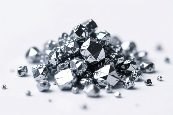
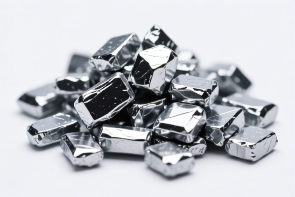
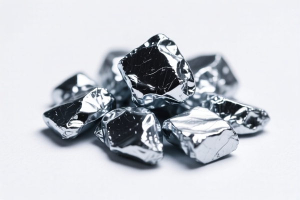
AI分析
🌌 High Purity Doped Silicon Wafers (The Heart of Modern Electronics)
🌐 HS Code Reference & Customs Clearance Guide | 2026 Latest Tariff Breakdown | Professional Clearance Strategy for Semiconductor Materials
📌 I. Product Definition & Classification: What Exactly is "Doped Silicon"?
High purity doped silicon wafers are the foundational substrate for semiconductor devices. They are not raw ore, nor are they finished chips. They are engineered materials where ultra-pure silicon crystals are infused with trace amounts of impurities (dopants like boron or phosphorus) to alter their electrical conductivity.
In international trade, classification hinges on two critical factors: 1. Chemical State: Is it just silicon (a chemical element)? Or is it a semiconductor device/component? 2. Process Stage: Is it a raw material ready for manufacturing (2804/3818)? Or is it a finished electrical component (8541)?
⚠️ Key Distinction:
- If the primary value is the material composition (silicon crystal structure + doping agent), it often falls under Chapter 28 (Inorganic Chemicals) or Chapter 38 (Miscellaneous Chemical Products).
- If the primary value is the electrical function (acting as a diode/transistor substrate), it may fall under Chapter 85 (Electrical Machinery).
- US Customs (CBP) tends to scrutinize "Doped" wafers heavily, often pushing them toward Chapter 85 if they are deemed "ready for use" in devices, but sometimes allowing Chapter 28 if classified as simple chemical commodities.
📦 II. HS Code Classification Details (2026 Latest Tariff Authority Match)
Based on the provided data, here are the 5 possible HS Codes for "High Purity Doped Silicon Wafers," ranging from raw chemical classification to finished semiconductor component.
| HS Code | Product Description | Applicability Scenario | Tax Logic & Explanation |
|---|---|---|---|
2804.69.10.00 |
Silicon (Other Forms) | Raw Silicon Material: Wafers considered as "other forms" of silicon, not specifically defined elsewhere. Fits the "catch-all" for silicon shapes. | 15.3% • Base: 5.3% • Additional: 0% • Section 301/122: 10% (Note: Lower additional tariff than some chemical codes) |
8541.59.00.40 |
Semiconductor Devices (Other) | Finished Component: Classified as a "semiconductor device" because the wafer is doped and ready for further processing into devices. Fits the "wafer" definition in Ch 85. | 10.0% • Base: 0.0% • Additional: 0.0% • Section 301/122: 10% (Note: Zero base duty makes this attractive if accepted) |
2804.61.00.00 |
Crystalline Silicon | Raw Crystal: Silicon in crystalline form, considered a "semi-finished" chemical product. Matches the explanation for "silicon pieces." | 60.0% • Base: 0.0% • Additional: 50.0% • Section 301/122: 10% (Note: HIGH RISK – 50% punitive tariff!) |
8541.10.00.40 |
Diodes (Chips/Wafers) | Electrical Component: Classified under diodes, specifically "uninstalled chips, grains, and wafers." Fits if the wafer is treated as a diode substrate. | 10.0% • Base: 0.0% • Additional: 0.0% • Section 301/122: 10% (Note: Similar to 8541.59, but specific to diode category) |
3818.00.00.20 |
Prepared Semiconductors | Doped Material: Specifically targets "doped" silicon. Matches "doped" characteristic and "polysilicon/wafer" form. | 60.0% • Base: 0.0% • Additional: 50.0% • Section 301/122: 10% (Note: HIGH RISK – 50% punitive tariff!) |
🔍 Critical Analysis:
- The "50% Trap": Codes2804.61.00.00and3818.00.00.20carry a 50% Additional Tariff (USITC Footnote). This is likely due to USITC restrictions on Chinese silicon materials. Avoid these if possible.
- The "Safe Zones": Codes2804.69.10.00,8541.59.00.40, and8541.10.00.40have significantly lower additional tariffs (0% or 10% only).
- The Dilemma: Customs may view "Doped" wafers as3818(prepared chemical) or8541(device). The argument for8541is that doping is an integral part of semiconductor device manufacturing, not just a chemical preparation.
💰 III. 2026 Latest Tariff Rate Breakdown (Including Surcharges)
✅ Applicable Country: United States (US)
✅ Origin: China (CN)
✅ Effective Time: Current 2025-2026 Trade Policy (Section 301 + IEEPA 122)
🎯 1. 2804.69.10.00 —— Silicon (Other Forms)
| Item | Content |
|---|---|
| Base Rate | 5.3% (ad valorem) |
| USITC Additional | 0.0% |
| IEEPA/Section 301 | +10% (China-specific surcharge) |
| Total Rate | 15.3% |
| Calculation | CIF Value × 15.3% |
| De Minimis | ❌ Not Eligible (deny_de_minimis) |
| Legal Path | IEEPA:9903.01.25 → USITC:2804.69.10.00 |
📌 Explanation:
- This code treats the wafer as a "shape" of silicon rather than a chemical compound or device.
- The 5.3% base rate is high, but the 0% additional USITC tariff makes it cheaper than2804.61or3818.
🎯 2. 8541.59.00.40 —— Semiconductor Devices (Other)
| Item | Content |
|---|---|
| Base Rate | 0.0% |
| USITC Additional | 0.0% |
| IEEPA/Section 301 | +10% (China-specific surcharge) |
| Total Rate | 10.0% |
| Calculation | CIF Value × 10.0% |
| De Minimis | ❌ Not Eligible |
| Legal Path | IEEPA:9903.01.24 → USITC:8541.59.00.40 |
📌 Explanation:
- Most Cost-Effective Option (if accepted).
- Argument: The wafer is a "semiconductor device" substrate. Doping is a manufacturing step, not a chemical preparation.
- Risk: CBP may argue it’s not a "device" yet, but a material.
🎯 3. 8541.10.00.40 —— Diodes (Wafers/Chips)
| Item | Content |
|---|---|
| Base Rate | 0.0% |
| USITC Additional | 0.0% |
| IEEPA/Section 301 | +10% (China-specific surcharge) |
| Total Rate | 10.0% |
| Calculation | CIF Value × 10.0% |
| De Minimis | ❌ Not Eligible |
| Legal Path | IEEPA:9903.01.24 → USITC:8541.10.00.40 |
📌 Explanation:
- Similar to above. If the wafer is specifically for diode manufacturing, this code is precise.
- Low base rate (0%) + Low surcharge (10%) = 10% Total.
🚫 4. 2804.61.00.00 & 3818.00.00.20 —— The High-Tax Traps
| Item | Content |
|---|---|
| Base Rate | 0.0% |
| USITC Additional | +50.0% (Critical!) |
| IEEPA/Section 301 | +10% |
| Total Rate | 60.0% |
| Calculation | CIF Value × 60.0% |
| De Minimis | ❌ Not Eligible |
📌 Warning:
- DO NOT USE unless absolutely forced by Customs.
- The 50% USITC tariff is a punitive measure against Chinese silicon materials.
-3818is often triggered if Customs views "doping" as a "preparation" rather than a "device manufacturing step."
🛠️ IV. Customs Clearance Practical Advice (Real-World Pitfall Guide)
✅ 1. Documentation Checklist (Non-Negotiable)
| Document | Required | Description |
|---|---|---|
| ✅ Product Specification Sheet | ✔️ | Must detail: Purity level (99.9999%+), Doping Type (Boron/Phosphorus), Resistivity, Wafer Thickness, Diameter (6", 8", 12"). |
| ✅ Material Safety Data Sheet (MSDS) | ✔️ | To prove chemical composition, but do not emphasize "chemical preparation" over "semiconductor application." |
| ✅ Technical Data Sheet (TDS) | ✔️ | Highlights electrical properties (n-type/p-type), proving it’s for electronic use, not industrial chemical use. |
| ✅ Commercial Invoice | ✔️ | Description must be precise: "Silicon Wafer, Doped, for Semiconductor Manufacturing, HS Code 8541.59.00.40." |
| ✅ Certificate of Origin | ✔️ | To verify China origin and apply IEEPA tariffs. |
| ✅ Bill of Lading | ✔️ | Consistent with invoice description. |
✅ 2. Declaration Strategy (Key Mantras)
🔥 “Focus on Function, Not Just Form!”
| Scenario | Correct Declaration | Wrong Practice |
|---|---|---|
| Doped Wafer for ICs | 8541.59.00.40 (Semiconductor Device) |
Calling it "Silicon Chemical" → Leads to 3818 (60% Tax) |
| Raw Crystal Silicon | 2804.61.00.00 |
Calling it "Wafer" if it’s just a crystal chunk |
| Polysilicon for Solar | 3818.00.00.20 (Check for exemptions) |
Using 8541 if it’s not for electronics |
| Uninstalled Wafer | 8541.10.00.40 or 8541.59.00.40 |
Calling it "Diode" if it’s not processed into a diode yet |
✅ 3. Special Handling Tips
| Situation | Handling Advice |
|---|---|
| Customs Audits "Doping" | Provide technical evidence that doping is an integral part of semiconductor device fabrication, not a chemical mixing process. Argue for 8541. |
| High Value/High Volume | Apply for a Binding Ruling (Pre-Decision) from CBP. Cost is worth avoiding 50% retroactive penalties. |
| Mixed Shipments | Clearly separate "Raw Silicon" (2804) from "Doped Wafers" (8541) in invoices. Mixing can trigger audits. |
| USITC Footnote Challenges | If CBP pushes 3818, appeal with Exclusion Letters (if any apply to your specific product code) or technical manuals proving electronic application. |
🌍 V. Global Market Comparison (2026 Latest)
| Country/Region | Recommended HS Code | Total Tariff | Certification | Note |
|---|---|---|---|---|
| 🇺🇸 United States | 8541.59.00.40 |
10.0% | FCC (if applicable), No CCC | Avoid 3818 (60%)! |
| 🇨🇳 China (Import) | 3818.00.00.20 |
~0-10% | CCC (if applicable) | Lower tariffs for domestic use |
| 🇪🇺 European Union | 3818.00.00.10 |
0% | REACH | No punitive tariffs like US |
| 🇯🇵 Japan | 3818.00.00.10 |
0% | PSE | Free trade agreements may apply |
| 🇰🇷 South Korea | 3818.00.00.10 |
0% | KC | Low tariff environment |
📌 Conclusion:
- The US is the only market with extreme tariffs on silicon materials.
- Strategy: Always argue for Chapter 85 (8541) to avoid the 50% USITC penalty on Chapter 28/38.
- Documentation is Key: Your TDS must scream "Electronics," not "Chemistry."
📌 VI. Common Mistakes & Pitfall Guide (Blood & Tears)
❌ Mistake 1: Classifying "Doped Wafers" as 3818 (Prepared Semiconductors)
👉 Consequence: 60% Total Tax! (0% Base + 50% USITC + 10% IEEPA).
👉 Fix: Argue that doping is part of device manufacturing, not chemical preparation.
❌ Mistake 2: Calling "Wafers" "Silicon Crystals" (2804.61)
👉 Consequence: 60% Total Tax! Same USITC penalty applies to crystalline silicon imports from China.
👉 Fix: Use 8541 if for semiconductor use.
❌ Mistake 3: Missing the "Doped" Specification
👉 Consequence: Customs may default to 3818 or 2804 due to ambiguity.
👉 Fix: Explicitly state "Doped for Semiconductor Application" in the invoice.
❌ Mistake 4: Ignoring IEEPA 122 Surcharge
👉 Consequence: Even if base is 0%, the 10% IEEPA surcharge applies to ALL Chinese-origin electronics/semiconductors.
👉 Fix: Budget for the 10% minimum.
✅ Correct Approach:
"Silicon Wafer, Doped (N-Type), 200mm Diameter, for IC Manufacturing, HS Code 8541.59.00.40, Origin China"
🎯 VII. Conclusion: Precision is Profit!
🎯 Remember the Mantra:
🔹 "Don't be a Chemical, Be a Device!"
🔹 "Chapter 85 saves 50%; Chapter 38/28 costs 50%!"
🔹 "10% is cheap; 60% is a death sentence!"
📌 Pro Tip:
If your wafer is originally sourced from the US, Japan, or Germany, you may still face IEEPA surcharges if processed in China. However, if you can prove substantial transformation in a third country (e.g., Vietnam, Thailand), you might avoid the 10% IEEPA tariff.
Always apply for a Pre-Ruling before your first shipment to lock in the 8541 classification.
📣 Take Action Now:
📞 Contact a customs broker specialized in semiconductors.
📄 Prepare your Technical Data Sheet highlighting "Electronic Application."
🚀 Lock in the 10% rate. Avoid the 60% trap.
✨ Professional Clearance Starts with Accurate Classification!
💼 Your Silicon Wafers are Precious. Protect Your Margins!
用户评价
关于 HS 编码归类
协调制度(HS)是由世界海关组织(WCO)制定的国际贸易商品分类标准。全球 200 多个国家采用 HS 系统作为海关关税、贸易统计和进出口监管的基础。
每个 HS 编码遵循以下层级结构:
- 章(2 位)——商品大类(例如:第 84 章:机器和机械设备)
- 品目(4 位)——章内的更具体分类
- 子目(6 位)——国际通用细分,所有 WCO 成员国统一使用
- 本国细分(8-10 位)——各国自行扩展的细分编码,如美国 HTSUS 10 位编码
正确的 HS 编码归类对于顺利通关、准确缴纳关税和遵守贸易法规至关重要。错误归类可能导致海关延误、多缴关税或罚款。
从CN进口到US时,适用的关税税率可能包括:
- 最惠国(MFN)税率——适用于 WTO 成员国的标准关税税率
- 普通税率——适用于无贸易协定国家
- 贸易救济关税——附加关税,如 301 条款(反倾销)、232 条款(国家安全)或反补贴税
本页内容仅供参考。如需正式归类,请咨询当地海关或持牌报关代理。