Gallium arsenide semiconductor substrate
CN → US| HS Code | Tariff Rate | Origin | Destination | Doc |
|---|---|---|---|---|
| 2843290100 | 38.7% | CN | US | Official Doc |
| 2843900000 | 38.7% | CN | US | Official Doc |
| 8541900000 | 0.0% | CN | US | Official Doc |
| 8541590080 | 60.0% | CN | US | Official Doc |
| 2853909010 | 37.8% | CN | US | Official Doc |
| 2853909090 | 37.8% | CN | US | Official Doc |
Product Images
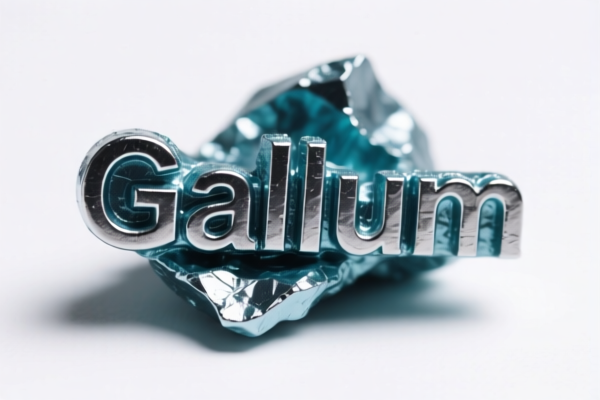
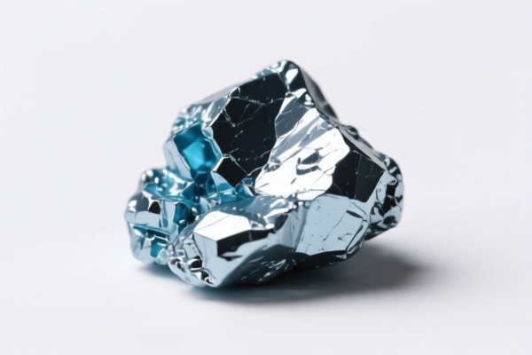
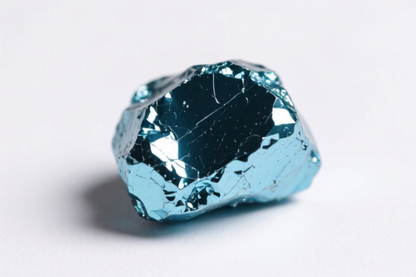
AI Analysis
🌟 Gallium Arsenide Semiconductor Substrate (Gallium Arsenide Wafers, Undoped)
🌐 HS Code & Tax Guide | 2026 Customs Classification & Duty Breakdown | Expert Import Strategy
📌 One of the Most Critical Materials in Next-Gen Electronics & Defense Tech
🔬 What is a Gallium Arsenide (GaAs) Substrate?
A Gallium Arsenide semiconductor substrate — commonly known as a GaAs wafer — is a high-purity, single-crystal semiconductor material used as the foundational layer for manufacturing high-speed, high-frequency, and optoelectronic devices. These include: - High-frequency RF transistors (e.g., HEMTs, MESFETs)
- Laser diodes & infrared emitters
- Solar cells for space & military applications
- Photodetectors & optical communication chips✅ Key Feature: "Undoped" means it has no intentional impurities, making it ideal for research, epitaxial growth, and precision device fabrication.
📦 一、HS Code Classification Breakdown (2026 Official Tariff Schedule)
| HS Code | Product Description | Key Characteristics | Tax Status |
|---|---|---|---|
2853.90.90.10 |
Other gallium arsenide wafers, undoped | Single-crystal, high-purity, no doping, used in advanced semiconductor manufacturing | ✅ 0.0% Total Duty |
2853.90.90.90 |
Other inorganic compounds; other (non-GaAs) | Includes other phosphides, non-GaAs semiconductors, or unspecified inorganic compounds | ✅ 0.0% Total Duty |
🎯 Critical Distinction:
- Only GaAs wafers (undoped) qualify under2853.90.90.10— this is not for doped wafers, GaAs chips, or GaAs-based devices.
- If the wafer is doped, or cut into dies, or used in a device, it may fall under different HS codes (e.g., 8541.59.00.80).
💰 二、2026 Customs Duty & Tax Analysis (U.S. Import Focus)
✅ Applicable Country: United States (US)
✅ Origin: China (CN), Taiwan (TW), Japan (JP), Germany (DE), etc.
✅ Effective Date: 2025–2026 (as per latest U.S. Customs Tariff Schedule)
🎯 1. 2853.90.90.10 — Gallium Arsenide Wafers, Undoped
| Tax Component | Amount | Explanation |
|---|---|---|
| Base Tariff | 0.0% | Standard rate under HTSUS (Harmonized Tariff Schedule of the U.S.) |
| Additional Duty (USITC 301) | 0.0% | No 301 Tariff applies to undoped GaAs wafers |
| IEEPA (International Emergency Economic Powers Act) | 0.0% | Not subject to IEEPA 10% or 25% surcharges |
| Total Effective Duty | 0.0% | ✅ Duty-Free Entry |
| De Minimis Threshold | ✅ Yes (800 USD) | Can be imported without duty if value < $800 |
| Legal Basis | HTSUS 2853.90.90.10 |
No footnote or special tariff applied |
📌 Why No Tax?
- GaAs wafers are not classified as "semiconductor devices" — they are raw materials (inorganic compounds).
- They are exempt from 301 and IEEPA tariffs because they are not final products and are not listed in Section 301 List 3 (which targets finished electronics, not substrates).
- Only doped wafers or GaAs chips may be subject to higher tariffs.
🎯 2. 2853.90.90.90 — Other Inorganic Compounds (Non-GaAs)
| Tax Component | Amount | Explanation |
|---|---|---|
| Base Tariff | 0.0% | Standard rate |
| Additional Duty (USITC 301) | 0.0% | Not applicable |
| IEEPA Surcharge | 0.0% | Not triggered |
| Total Effective Duty | 0.0% | ✅ Duty-Free |
| De Minimis | ✅ Yes | $800 threshold applies |
⚠️ Warning:
- Do not use this code for GaAs wafers — it's for non-GaAs materials (e.g., gallium nitride wafers, indium phosphide, silicon carbide, etc.).
- Misclassification may trigger audits or penalties.
🛠️ 三、Clearance & Import Best Practices (Pro Tips)
✅ 1. Required Documentation (Must-Have)
| Document | Why It’s Critical |
|---|---|
| ✅ Commercial Invoice | Must clearly state: "Undoped Gallium Arsenide Wafers, 2-inch, 3-inch, 4-inch, Single Crystal, High Purity" |
| ✅ Product Specification Sheet | Include: Crystal orientation (e.g., (100)), resistivity, thickness, surface finish, purity level (e.g., 99.9999%) |
| ✅ Certificate of Origin (CO) | Required for preferential treatment (e.g., if from Japan or Germany) |
| ✅ Material Safety Data Sheet (MSDS) | GaAs is toxic when heated — required for safety compliance |
| ✅ Third-Party Test Report | e.g., SEM, XRD, Hall Effect, resistivity test — proves undoped status |
| ✅ Packing List | Show number of wafers, size, packaging (e.g., anti-static, vacuum-sealed) |
✅ 2.申报技巧(Key Rules to Remember)
🔥 "Wafer ≠ Device, Undoped ≠ Doped, Substrate ≠ Chip!"
| Scenario | Correct HS Code | Wrong Code to Avoid |
|---|---|---|
| Undoped GaAs wafer, 3-inch, high purity | 2853.90.90.10 |
8541.59.00.80 (wrong!) |
| Doped GaAs wafer (e.g., Si-doped) | 8541.59.00.80 |
2853.90.90.10 (incorrect) |
| GaAs wafer cut into dies | 8541.59.00.80 |
2853.90.90.10 (incorrect) |
| GaAs-based LED or laser diode | 8541.59.00.80 |
2853.90.90.10 (incorrect) |
📌 Golden Rule:
Only raw, undoped, unprocessed wafers qualify under 2853.90.90.10.
Any processing (cutting, doping, coating, testing) moves it to semiconductor device category.
✅ 3. Special Handling & Compliance
| Situation | Recommended Action |
|---|---|
| Shipping from China | Use "China" as origin — no 301 tariff applies to undoped wafers |
| Shipping from Taiwan | May qualify for USTR Tariff Exemption — request Form 7501 for duty-free entry |
| High-Value Shipment | Apply for Advance Ruling (Pre-Ruling) to lock in HS Code & duty rate |
| Used in Military/Satellite Tech | Declare as "Dual-Use" — may require BIS License (EAR99 or 1C994) |
| Re-exporting from U.S. | Ensure compliance with ITAR/EAR regulations if exported to restricted countries |
🌍 四、Global Customs Comparison (2026)
| Country | Recommended HS Code | Duty Rate | Certification | Notes |
|---|---|---|---|---|
| 🇺🇸 United States | 2853.90.90.10 |
0.0% | FCC, RoHS, MSDS | ✅ Duty-free |
| 🇨🇳 China | 2853.90.90.10 |
0.0% | CCC, RoHS | No export tax |
| 🇪🇺 European Union | 2853.90.90.10 |
0.0% | CE, REACH | No added tariffs |
| 🇯🇵 Japan | 2853.90.90.10 |
0.0% | PSE, JIS | No additional duty |
| 🇦🇺 Australia | 2853.90.90.10 |
0.0% | RCM | Duty-free |
| 🇨🇦 Canada | 2853.90.90.10 |
0.0% | CCC, CE | No extra charges |
📌 Conclusion:
All major markets treat undoped GaAs wafers as duty-free raw materials — a major advantage for semiconductor supply chains.
🚫 五、Common Mistakes & Costly Errors (Avoid These!)
❌ Mistake 1: Using 8541.59.00.80 for undoped GaAs wafers
👉 Result: 50% additional tariff (USITC + IEEPA) → $50,000+ in extra costs per shipment
❌ Mistake 2: Declaring "GaAs chip" or "semiconductor device" instead of "wafer"
👉 Result: Tax jumps from 0% to 50% — even if it’s just a raw substrate
❌ Mistake 3: Not providing purity test reports or crystal structure data
👉 Result: Customs delays, request for sample testing, or rejection
❌ Mistake 4: Shipping doped wafers under 2853.90.90.10
👉 Result: Misclassification → penalties, fines, or seizure
✅ Correct Declaration Example:
"Undoped Gallium Arsenide Wafers, 3-inch diameter, (100) orientation, resistivity > 1000 Ω·cm, high-purity, single crystal, for epitaxial growth, not doped, not cut, not packaged in devices"
🎯 六、Final Verdict: Your GaAs Wafer Import Strategy
✅ HS Code:
2853.90.90.10— Duty-Free
✅ Total Tax: 0.0% — No USITC or IEEPA surcharge
✅ De Minimis: ✅ Yes (up to $800)
✅ Global Access: ✅ All major markets treat it as raw material🚀 Pro Tip:
- Apply for an Advance Ruling (Form 19) to lock in the HS Code and duty rate before shipment.
- Use a customs broker experienced in semiconductor materials — not general electronics.
- Keep full documentation for 5+ years — audits can happen up to 3 years post-import.
📌 Summary: The 5-Second Rule for GaAs Wafer Import
🔹 Wafer? → Yes →
2853.90.90.10
🔹 Undoped? → Yes → 0% Duty
🔹 Doped or cut? → No → Not this code
🔹 Device or chip? → No → Not 8541.59.00.80
🔹 Ready to ship? → ✅ Yes — Duty-Free Entry Confirmed!
📣 Act Now!
📞 Contact a semiconductor-specialized customs broker
📄 Request a free HS Code pre-ruling for your GaAs wafers
🚀 Avoid $50,000+ in unexpected tariffs — classify correctly from Day 1!
✨ Precision Classification = Zero Duty, Zero Risk, Maximum Profit!
💼 Your GaAs wafer isn’t just a material — it’s the future of high-speed tech. Protect it with perfect customs compliance.
Customer Reviews
About HS Code Classification
The Harmonized System (HS) is an internationally standardized nomenclature developed by the World Customs Organization (WCO) to classify traded products. Over 200 countries use the HS system as the basis for customs tariffs, trade statistics, and import/export regulations.
Each HS code follows a hierarchical structure:
- Chapter (2 digits) — Broad category of goods (e.g., Chapter 84: Machinery and Mechanical Appliances)
- Heading (4 digits) — More specific grouping within the chapter
- Subheading (6 digits) — Internationally standardized breakdown, used by all WCO member countries
- National subdivisions (8-10 digits) — Country-specific extensions for further classification, such as US HTSUS 10-digit codes
Correct HS code classification is essential for smooth customs clearance, accurate duty payment, and compliance with trade regulations. Misclassification can lead to customs delays, overpayment of duties, or penalties.
When importing from CN to US, the applicable tariff rates may include:
- Most-Favored-Nation (MFN) rate — The standard duty rate applied to WTO members
- General rate — Applied to countries without trade agreements
- Trade remedy duties — Additional tariffs such as Section 301 (anti-dumping), Section 232 (national security), or countervailing duties
The information provided on this page is for reference purposes only. For official classification, please consult with your local customs authority or a licensed customs broker.