Highly Doped Silicon Wafer
CN → US| HS Code | Tariff Rate | Origin | Destination | Doc |
|---|---|---|---|---|
| 2804691000 | 15.3% | CN | US | Official Doc |
| 8541100040 | 60.0% | CN | US | Official Doc |
| 8541590040 | 60.0% | CN | US | Official Doc |
| 3818000095 | 60.0% | CN | US | Official Doc |
| 3818000020 | 60.0% | CN | US | Official Doc |
| 2804610000 | 60.0% | CN | US | Official Doc |
Product Images
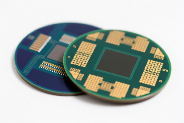
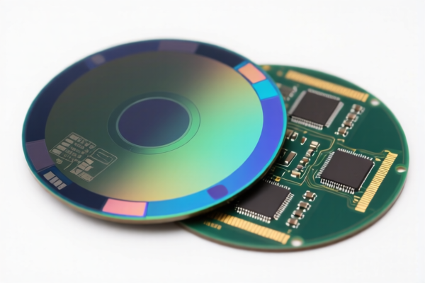
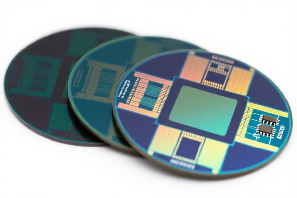
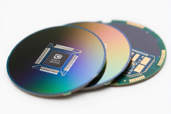
AI Analysis
⚛️ Highly Doped Silicon Wafer
🌐 HS Code Reference & Customs Clearance Guide | 2026 Latest Tariff Full Analysis | Professional Clearance Strategy
📌 I. Product Definition & Classification: Do You Truly Understand "Silicon Wafers"?
A Highly Doped Silicon Wafer is a critical semiconductor substrate. In international trade, its classification hinges on two key factors:
1. State of Processing: Is it a raw elemental material or a processed semiconductor component?
2. Functionality: Is it used as a passive material or an active electronic component?
⚠️ Critical Distinction:
- If it is considered a raw chemical material (elemental silicon with impurities for industrial use) →归类 to Chapter 28 (Inorganic Chemicals).
- If it is considered a semiconductor device/component (processed wafer/wafers for electronic use) → 归类 to Chapter 85 or Chapter 38 (Electrical Machinery/Semiconductors).
📦 II. HS Code Classification Details (2026 Latest Tariff Authority Comparison)
| HS Code | Product Description | Application Scenario | Tax Rate (Total) | Key Reasoning from DATA |
|--------|--------------------------|----------|----------------|
| 2804.69.10.00 | Other Silicon (Elemental Silicon, semi-finished form) | Raw silicon material, basic semiconductor substrate, non-electronic industrial use. | 15.3% | Match Success: The name "Silicon" matches the material requirement; "Wafer" is a semi-finished form, compatible with "Other Silicon".
🔹 Lowest Tax Option |
| 8541.10.00.40 | Uninstalled Chips, Dies, and Wafers (Semiconductor Materials) | Processed wafers (wafer state), doped silicon, used as active semiconductor material. | 60.0% | Match Basis: Form is "Silicon Wafer" (wafer state), material is "Doped Silicon" (semiconductor material); fits "Uninstalled chips, dies, and wafers". |
| 8541.59.00.40 | Other Semiconductor Devices (Unassembled Wafers) | Silicon wafers (wafers), silicon material, fits "Unassembled wafers" definition. | 60.0% | Match Basis: Form is "Silicon Wafer" (wafers), material is "Silicon" (semiconductor material); fits "Unassembled wafers". |
| 3818.00.00.95 | Cut Wafers (Other doped materials) | Cut wafers/discs, low-impedance doping, fits "Other doped materials" (excluding GaAs, Polysilicon, SiC). | 60.0% | Match Basis: Material "Silicon", form "Silicon Wafer" (disc/wafer), use "Low-impedance doping"; fits the residual category for other doped materials. |
| 3818.00.00.20 | Polysilicon Wafers, Doped | Doped silicon wafers, matches "Polysilicon wafers, doped" in material (Silicon) and use (Doping). | 60.0% | Match Success: "Doped Silicon Wafer" matches "Polysilicon wafers, doped" in material and use. |
| 2804.61.00.00 | Monosilicon (Elemental Silicon) | Silicon material, doped silicon wafer (semi-finished), fits material attribute definition. | 60.0% | Match Basis: Name "Silicon" matches material; "Doped Silicon Wafer" is semi-finished, fits material attribute definition, no conflict. |
🔍 Key Insight:
- There is a massive tax discrepancy between Chapter 28 (2804.69.10.00@ 15.3%) and Chapters 38/85 (all @ 60.0%).
- The core argument is whether the "Doped Silicon Wafer" is classified as a raw chemical product or a semiconductor component.
💰 III. 2026 Latest Tariff Rate Details (Including Surtaxes & Policy Add-ons)
✅ Applicable Country: United States (US)
✅ Origin: China (CN)
✅ Effective Time: From November 10, 2025 (including subsequent imports)
🎯 1. 2804.69.10.00 —— Other Silicon (Elemental Silicon)
🏆 BEST CASE SCENARIO: Lowest Tax Rate
| Item | Details |
|---|---|
| Base Tariff | 5.3% |
| USITC Surtax (Section 301) | +0.0% |
| 122 Clause Tariff (IEEPA) | +10.0% |
| Total Tariff Rate | 15.3% |
| De Minimis Exemption | ❌ Not Eligible (Deny De Minimis for China-origin goods under Section 301/IEEPA usually applies to higher value, but specific footnotes may apply; however, 15.3% is still significantly lower than 60%) |
| Legal Basis Path | USITC:2804.69.10.00 → FOOTNOTE:301/122 |
📌 Explanation:
- This classification treats the wafer as a chemical element (silicon) in a semi-finished state.
- Significant Cost Advantage: 15.3% vs. 60%.
- Risk: US Customs may reclassify it as a semiconductor if "doping" implies electronic function.
🎯 2. 8541.10.00.40 / 8541.59.00.40 / 3818.00.00.95 / 3818.00.00.20 / 2804.61.00.00
⚠️ HIGH TAX SCENARIO: Semiconductor/Component Classification
| Item | Details |
|---|---|
| Base Tariff | 0.0% (Most Chapter 85/38 items have 0% base) |
| USITC Surtax (Section 301) | +50.0% |
| 122 Clause Tariff (IEEPA) | +10.0% |
| Total Tariff Rate | 60.0% |
| De Minimis Exemption | ❌ Not Eligible |
| Legal Basis Path | USITC:8541.10.00.40 → FOOTNOTE:9903.88.01 / IEEPA:9903.01.25 → IEEPA:9903.01.24 |
📌 Explanation:
- 50% Section 301 Surtax: Applies to semiconductor devices and related materials from China.
- 10% IEEPA Surtax: Additional tariff under International Emergency Economic Powers Act.
- Total 60%: This is a prohibitive tax rate for many businesses.
🛠️ IV. Customs Clearance Practical Advice (Real-World Pitfall Avoidance Guide)
✅ 1. Preparation Checklist (Must-Haves)
| Material | Must Provide | Explanation |
|---|---|---|
| ✅ Product Specification Sheet | ✔️ | Detail doping concentration, resistivity, crystal orientation (e.g., <100>, <111>), diameter, thickness. |
| ✅ Technical Data Sheet (TDS) | ✔️ | Prove if it is used as a substrate (passive) or active semiconductor. |
| ✅ Product Photos (Clear) | ✔️ | Show surface quality, packaging, and any markings. |
| ✅ Certificate of Analysis (COA) | ✔️ | Confirm purity and doping levels. |
| ✅ Commercial Invoice | ✔️ | Clearly state "Silicon Wafer" vs. "Semiconductor Device". Avoid vague terms like "Chip". |
| ✅ Packing List | ✔️ | Ensure consistency with invoice. |
✅ 2. Declaration Strategy (Key Mnemonics)
🔥 “Low Resistivity = Chemical, High Precision = Semiconductor!”
| Scenario | Recommended HS Code | Risk Level |
|---|---|---|
| General Industrial Silicon Wafers (High resistivity, low doping, used as substrate) | 2804.69.10.00 |
✅ Low Risk (15.3%) |
| Highly Doped/Low Resistivity Wafers (Used for specific electronic devices, MEMS, sensors) | 8541.10.00.40 or 3818.00.00.95 |
⚠️ High Risk (60%) |
Polysilicon Wafers (Specifically mentioned in 3818.00.00.20) |
3818.00.00.20 |
⚠️ High Risk (60%) |
| Monocrystalline Silicon (If argued as raw material) | 2804.61.00.00 |
⚠️ High Risk (60% - Note: DATA shows 60% for this code due to surtaxes) |
📌 Crucial Note:
- Do NOT declare as "Silicon Wafer" if it is clearly a finished semiconductor component.
- If it is Highly Doped (Low Resistivity), US Customs is likely to classify it under Chapter 85 or 38, triggering the 60% tax.
- Argument for 15.3%: Emphasize that the wafer is a raw material for further manufacturing, not a finished electronic component.
✅ 3. Special Case Handling
| Situation | Handling Advice |
|---|---|
| Doping Level is Low | Provide COA showing high resistivity → Argue for 2804.69.10.00 (15.3%). |
| Doping Level is High (Low Resistivity) | Expect 60% tax. Consider supply chain restructuring if possible. |
| Polysilicon vs. Monosilicon | 3818.00.00.20 explicitly covers "Polysilicon Wafers, Doped". Monosilicon may have more argument space for 2804 but still risky. |
| Pre-Ruling | Highly Recommended! File an Advance Ruling with US Customs to confirm HS Code before shipment. |
🌍 V. Global Market Comparison (2026 Latest)
| Country/Region | Recommended HS Code | Tariff (China Origin) | Certification | Note |
|---|---|---|---|---|
| 🇺🇸 USA | 2804.69.10.00 |
15.3% | None | Best Case8541/3818: 60% |
| 🇺🇸 USA | 8541.10.00.40 |
60.0% | None | Worst Case |
| 🇪🇺 EU | 2804.69 |
Varies (Look for Free Trade Agreements) | CE, RoHS | EU may treat silicon wafers as raw materials. |
| 🇨🇳 China | 2804.69 |
5% (Import Duty) | None | Lower baseline tax. |
📌 Conclusion:
- USA is the most challenging market due to the 44.7% tariff gap (15.3% vs. 60%).
- China-origin silicon wafers face significant tariffs if classified as semiconductors.
📌 VI. Common Mistakes & Pitfall Avoidance (Blood & Tears Lessons)
❌ Mistake 1: Declaring "Highly Doped Silicon Wafer" as 2804.69.10.00 without justification.
👉 Consequence: Customs reclassifies to 8541 or 3818 → Back taxes + Penalties (44.7% difference).
❌ Mistake 2: Using vague description "Silicon Material".
👉 Consequence: Customs demands detailed specs → Delays or forced classification to highest tax rate.
❌ Mistake 3: Ignoring the "Doping" aspect.
👉 Consequence: "Doped" implies electronic function → Pushes classification toward Chapter 85/38.
❌ Mistake 4: Assuming all Silicon Wafers are the same.
👉 Consequence: Polysilicon, Monosilicon, and Doped wafers have different HS codes and tax implications.
✅ Correct Practice:
“Monocrystalline Silicon Wafer, Undoped/Weakly Doped, Resistivity > 10 Ohm-cm, for Semiconductor Substrate Use, Model XYZ, Diameter 150mm”
(Use this description to argue for2804.69.10.00)
🎯 VII. Conclusion: Professional Declaration Saves Money!
🎯 Remember the Mnemonic:
🔹 “Low Resistivity = 60%, High Resistivity = 15.3%!”
🔹 “Doping = Semiconductor, Raw Silicon = Chemical!”
🔹 “Pre-Ruling is King, Avoid 60% Tax Trap!”
📌 Pro Tip:
If your silicon wafers are highly doped and intended for electronic use, the 60% tariff is likely unavoidable under current US trade policies. Consider:
1. Advance Ruling: Get official confirmation from US CBP.
2. Supply Chain Diversification: Explore sourcing from non-China origins to mitigate Section 301/IEEPA tariffs.
3. Technical Argument: If possible, demonstrate that the wafer is a raw material with minimal electronic function to argue for 2804.69.10.00.
📣 Immediate Action:
📞 Contact a Customs Broker + Provide Doping Specs + File for Advance Ruling
🚀 Ensure Smooth Clearance, Minimize Tax Liability, Maximize Profit!
✨ Professional Clearance Starts with Accurate Classification!
💼 Every Cent of Cost Deserves Precise Calculation!
Customer Reviews
About HS Code Classification
The Harmonized System (HS) is an internationally standardized nomenclature developed by the World Customs Organization (WCO) to classify traded products. Over 200 countries use the HS system as the basis for customs tariffs, trade statistics, and import/export regulations.
Each HS code follows a hierarchical structure:
- Chapter (2 digits) — Broad category of goods (e.g., Chapter 84: Machinery and Mechanical Appliances)
- Heading (4 digits) — More specific grouping within the chapter
- Subheading (6 digits) — Internationally standardized breakdown, used by all WCO member countries
- National subdivisions (8-10 digits) — Country-specific extensions for further classification, such as US HTSUS 10-digit codes
Correct HS code classification is essential for smooth customs clearance, accurate duty payment, and compliance with trade regulations. Misclassification can lead to customs delays, overpayment of duties, or penalties.
When importing from CN to US, the applicable tariff rates may include:
- Most-Favored-Nation (MFN) rate — The standard duty rate applied to WTO members
- General rate — Applied to countries without trade agreements
- Trade remedy duties — Additional tariffs such as Section 301 (anti-dumping), Section 232 (national security), or countervailing duties
The information provided on this page is for reference purposes only. For official classification, please consult with your local customs authority or a licensed customs broker.