Monocrystalline Silicon Wafer
CN → US| HS Code | Tariff Rate | Origin | Destination | Doc |
|---|---|---|---|---|
| 2804610000 | 60.0% | CN | US | Official Doc |
| 8541491010 | 60.0% | CN | US | Official Doc |
| 8541100040 | 60.0% | CN | US | Official Doc |
| 2804691000 | 15.3% | CN | US | Official Doc |
| 3824991900 | 41.5% | CN | US | Official Doc |
Product Images
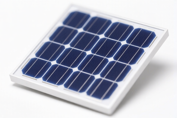
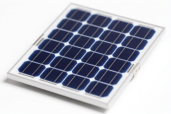
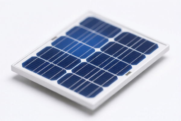
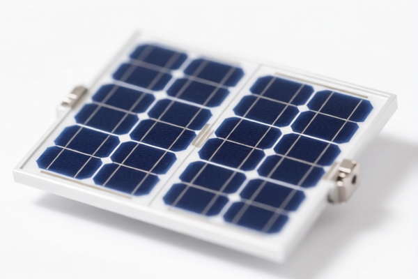
AI Analysis
💎 Monocrystalline Silicon Wafer (单晶硅片)
🌐 HS Code Reference & Customs Clearance Guide | 2026 Latest Tariff Analysis | Professional Tier-1 Strategy
📌 I. Product Definition & Classification: What Exactly Is a "Silicon Wafer"?
Monocrystalline Silicon Wafers are the foundational raw materials for the semiconductor industry, serving as the substrate for integrated circuits, solar cells, and optoelectronic devices. In international trade, classification depends heavily on the purity level, physical form (bulk crystal vs. processed wafer), and intended use (semiconductor device manufacturing vs. raw material processing).
The critical distinction lies between: 1. Raw/Processed Silicon Material: Classified under Chapter 28 (Inorganic Chemicals), focusing on the material itself. 2. Semiconductor Substrates/Uninstalled Chips: Classified under Chapter 85 (Electrical Machinery), focusing on the electronic function or form factor (wafer/die) ready for device fabrication.
⚠️ Key Classification Triggers:
- If declared as "Raw Silicon Material" (bulk, unprocessed or simply cut): Likely falls under 2804.61/2804.69.
- If declared as "Semiconductor Wafers/Dies" (processed, polished, specific electronic grade): Likely falls under 8541.49/8541.10.
- Conflict Alert: Misclassification between Chapter 28 and Chapter 85 can lead to significant tariff discrepancies (15.3% vs. 60.0%).
📦 II. HS Code Classification Details (2026 Authoritative Mapping)
Based on the provided data, here is the detailed breakdown of potential HS Codes for Monocrystalline Silicon Wafers:
| HS Code | Product Description | Application Scenario | Material/Form Characteristic |
|---|---|---|---|
| 2804.61.00.00 | Monocrystalline silicon slices/wafers; Material is Silicon; Form is slice or monocrystalline wafer. | Bulk silicon processing; Raw material supply for further chemical processing. | ✅ Inorganic Chemical Focus |
| 8541.49.10.10 | Monocrystalline silicon wafer classified as semiconductor material; Uninstalled chips, dies, and wafers. | High-purity semiconductor manufacturing substrate; Ready for IC fabrication. | ✅ Electronic Component Focus |
| 8541.10.00.40 | Monocrystalline silicon wafer as primary form of semiconductor material (Wafer); Uninstalled chips/dies definition. | Standard semiconductor wafer supply for front-end manufacturing. | ✅ Electronic Component Focus |
| 2804.69.10.00 | Silicon monocrystalline wafer; Material is Silicon; Form is slice; Processed form of Silicon. | Intermediate processed silicon; Non-specialized electronic grade or lower purity. | ✅ Inorganic Chemical Focus |
| 3824.99.19.00 | Silicon monocrystalline wafer as monocrystalline form; Matches "grown crystal" material/form; No chemical制剂 conflict. | Specialty crystals; Non-standard electronic applications or specific industrial crystals. | ✅ Miscellaneous Chemical Focus |
🔍 Critical Distinction:
- Chapter 28 (2804): Treats the wafer as a chemical product (silicon). Lower base tariff, but still subject to additional duties.
- Chapter 85 (8541): Treats the wafer as a semiconductor component/substrate. Highest tax burden due to "122 Clause" and Section 301/IEEPA implications.
- Chapter 38 (3824): Used for less common or specialized crystal forms not fitting standard chemical or electronic definitions precisely.
💰 III. 2026 Latest Tariff Rate Breakdown (Including Surcharge & Policy Add-ons)
✅ Applicable Country: United States (US)
✅ Origin: China (CN)
✅ Effective Date: Current trade policies include Section 301 and IEEPA surcharges.
🎯 1. 8541.49.10.10 & 8541.10.00.40 —— Semiconductor Wafers / Uninstalled Chips
| Item | Detail |
|---|---|
| Base Tariff | 0.0% (ad valorem) |
| Section 301 / Additional Surcharge | +50.0% |
| 122 Clause Tariff | +10.0% |
| Total Effective Rate | 60.0% |
| Tax Calculation | CIF Value × 60% |
| De Minimis Exemption | ❌ NOT ELIGIBLE (High-value semiconductor components are strictly regulated) |
| Legal Basis Path | USITC:8541.49.10.10 / 8541.10.00.40 → Section 301: 50% → 122 Clause: 10% |
📌 Explanation:
- These codes classify the wafer as a semiconductor material/component.
- The 50% additional tariff is the dominant cost driver, reflecting US restrictions on advanced semiconductor supply chains.
- The 10% "122 Clause" tariff is a specific anti-dumping or countervailing duty often applied to Chinese semiconductor materials.
- Total 60% is extremely high. Importers must carefully verify if the wafer truly qualifies for Chapter 85 (electronic function) vs. Chapter 28 (raw material).
🎯 2. 2804.61.00.00 —— Monocrystalline Silicon Slices (Raw Material)
| Item | Detail |
|---|---|
| Base Tariff | 0.0% (ad valorem) |
| Section 301 / Additional Surcharge | +50.0% |
| 122 Clause Tariff | +10.0% |
| Total Effective Rate | 60.0% |
| Tax Calculation | CIF Value × 60% |
| De Minimis Exemption | ❌ NOT ELIGIBLE |
| Legal Basis Path | USITC:2804.61.00.00 → Section 301: 50% → 122 Clause: 10% |
📌 Explanation:
- Even if classified as a chemical raw material, silicon wafers of this specific form are heavily scrutinized.
- Surprisingly, the total rate remains 60.0% due to the same additional tariffs applying to silicon-based inputs in the semiconductor sector.
- Strategic Note: While the rate is the same, the description and compliance requirements differ. Chapter 28 requires chemical purity specs; Chapter 85 requires electronic grade specs.
🎯 3. 2804.69.10.00 —— Processed Silicon Slices (Non-Specific Grade)
| Item | Detail |
|---|---|
| Base Tariff | 5.3% (ad valorem) |
| Section 301 / Additional Surcharge | 0.0% (No additional surcharge listed in data) |
| 122 Clause Tariff | +10.0% |
| Total Effective Rate | 15.3% |
| Tax Calculation | CIF Value × 15.3% |
| De Minimis Exemption | ❌ NOT ELIGIBLE (Likely still subject to restrictions) |
| Legal Basis Path | USITC:2804.69.10.00 → 122 Clause: 10% |
📌 Explanation:
- This code represents "Other Silicon" (not specific monocrystalline slices under 2804.61).
- Lower Base Rate (5.3%) and No 50% Section 301 Surcharge make this significantly cheaper.
- However: This classification is risky. Customs may challenge if the wafer is clearly intended for semiconductor use, reclassifying it to 8541 (60%) or 2804.61 (60%). Use only if the wafer is not for electronic semiconductor purposes (e.g., solar grade, industrial chemical use).
🎯 4. 3824.99.19.00 —— Grown Crystals / Specialty Materials
| Item | Detail |
|---|---|
| Base Tariff | 6.5% (ad valorem) |
| Section 301 / Additional Surcharge | +25.0% |
| 122 Clause Tariff | +10.0% |
| Total Effective Rate | 41.5% |
| Tax Calculation | CIF Value × 41.5% |
| De Minimis Exemption | ❌ NOT ELIGIBLE |
| Legal Basis Path | USITC:3824.99.19.00 → Section 301: 25% → 122 Clause: 10% |
📌 Explanation:
- Classified under "Miscellaneous Chemical Products" as "grown crystals."
- Moderate Risk: Higher than 2804.69 (15.3%) but lower than 8541/2804.61 (60%).
- Suitable for non-standard silicon forms or specialty crystals not fitting standard semiconductor or chemical wafer definitions.
🛠️ IV. Customs Clearance Practical Advice (Avoiding Pitfalls)
✅ 1. Document Checklist (Non-Negotiable)
| Document | Required? | Purpose |
|---|---|---|
| ✅ Technical Specification Sheet | ✔️ | Defines purity (9N, 6N, etc.), diameter, thickness, orientation. Critical for Chapter 28 vs. 85. |
| ✅ Certificate of Analysis (CoA) | ✔️ | Proves material properties. Required to justify "Raw Material" vs. "Semiconductor Component." |
| ✅ End-Use Statement | ✔️ | Must clearly state: "For semiconductor device fabrication" (→ 8541) or "For solar/industrial use" (→ 2804). |
| ✅ Product Photos | ✔️ | Clear images of the wafer, including any markings (dopant type, orientation flat). |
| ✅ Commercial Invoice | ✔️ | Must match HS Code description exactly. No vague terms like "Silicon Piece." |
| ✅ Packing List | ✔️ | Details quantity, weight, and packaging type. |
✅ 2. Classification Strategy (Key Decision Tree)
🔥 "Define Intent, Choose Chapter, Avoid 60% Trap!"
| Scenario | Recommended HS Code | Total Tariff | Risk Level |
|---|---|---|---|
| Semiconductor Grade Wafer (For ICs, Chips) | 8541.49.10.10 or 8541.10.00.40 |
60.0% | ⚠️ High Cost (Justify electronic function) |
| Raw Silicon Slice (For further processing) | 2804.61.00.00 |
60.0% | ⚠️ High Cost (Same rate, different docs) |
| Solar/Industrial Grade (Lower purity) | 2804.69.10.00 |
15.3% | ✅ Low Cost (Prove non-semiconductor use) |
| Specialty Crystal (Non-standard) | 3824.99.19.00 |
41.5% | ⚠️ Medium Risk (Customs may challenge) |
📌 Critical Warning:
- Do NOT use2804.69.10.00(15.3%) for high-purity semiconductor wafers. Customs will likely reclassify to8541(60%) and impose penalties.
- If the wafer is polished, doped, and sized for IC manufacturing, it is almost certainly8541.
- If the wafer is cut but not polished, or for solar cells, it may qualify for2804.61or2804.69, but note that2804.61still carries the 60% rate.
✅ 3. Special Handling Tips
| Situation | Advice |
|---|---|
| OEM/Custom Wafers | Provide customer specifications and design documents. Justify why it fits a specific code. |
| Mixed Shipments | Do not mix semiconductor-grade wafers (8541) with solar-grade (2804.69) in one line item. Declare separately. |
| Wafer Carriers (FOUPs) | If shipped with carriers, declare the wafer as the primary good. Carriers may be classified separately (8541.90), but ensure the wafer's classification is primary. |
| Origin Marking | Ensure "Made in China" is clearly marked on packaging to avoid tariff evasion suspicions. |
🌍 V. Global Market Comparison (2026 Context)
| Market | Recommended HS Code | Approx. Tariff (China Origin) | Key Certification | Notes |
|---|---|---|---|---|
| 🇺🇸 USA | 8541.49.10.10 / 8541.10.00.40 |
60.0% | FCC (if applicable), No specific Wafer Cert | Highest Barrier. Strict surveillance on semiconductor inputs. |
| 🇪🇺 EU | 3818.00.19 / 8541.49 |
0% - 6% | CE, RoHS | Favorable. Lower base tariffs. Focus on chemical safety. |
| 🇨🇳 China | 3818.00 / 2804.61 |
0% - 5% | CCC (if applicable) | Lowest Barrier. Encourages domestic semiconductor supply chain. |
| 🇯🇵 Japan | 3818.00 / 8541.49 |
0% - 8% | PSE, JIS | Moderate. High quality standards. |
📌 Conclusion:
- The USA is the most challenging market due to 60% effective tariffs and strict Section 301/122 Clause enforcement.
- For US imports, cost optimization is nearly impossible without origin shifting or product re-engineering (e.g., shipping as raw silicon chunks instead of wafers, if feasible).
- EU and Asia offer significantly lower tariff barriers, making them more attractive for non-US markets.
📌 VI. Common Mistakes & Pitfalls (Lessons Learned)
❌ Mistake 1: Declaring "Semiconductor Wafer" as "Silicon Metal" to get lower tariffs.
👉 Consequence: Customs audit reveals electronic-grade specs → Reclassified to 8541 (60%) + Penalties + Back Taxes.
❌ Mistake 2: Ignoring the "122 Clause" in documentation.
👉 Consequence: Customs demands proof of exemption → Shipment held for weeks → Demurrage Costs.
❌ Mistake 3: Using generic descriptions like "Silicon Wafer" without purity grades.
👉 Consequence: Customs cannot determine the correct code → Manual examination → Delay + Higher Duty Assessment.
✅ Correct Practice:
"Monocrystalline Silicon Wafer, 200mm, P-Type, 1-10 Ohm-cm, Electronic Grade, for IC Substrate, Model XYZ, Purity 9N+"
🎯 VII. Conclusion: Strategic Compliance for Silicon Wafers
🎯 Key Takeaway:
🔹 "60% is the Semiconductor Tax: If it's for chips, pay the price."
🔹 "15.3% is the Raw Material Escape: Only for non-electronic, industrial-grade silicon."
🔹 "Documentation is Key: Purity, Grade, and End-Use must align perfectly with the HS Code."
📌 Pro Tip:
If you are importing into the USA, consider Advance Rulings from CBP to lock in the classification. If the wafer is solar-grade, explicitly state "For Photovoltaic Cell Manufacturing" to potentially use 2804.69 (15.3%) instead of 8541 (60%). Never gamble on classification for high-value semiconductor inputs.
📣 Immediate Action:
📞 Consult a Customs Broker + Provide Technical Data Sheets + Apply for Pre-Ruling
🚀 Ensure Smooth Clearance, Avoid 60% Shock, Protect Margins!
✨ Precision in Classification is Profit in Your Pocket!
💼 Every Silicon Wafer is a Strategic Asset – Handle it with Care!
Customer Reviews
About HS Code Classification
The Harmonized System (HS) is an internationally standardized nomenclature developed by the World Customs Organization (WCO) to classify traded products. Over 200 countries use the HS system as the basis for customs tariffs, trade statistics, and import/export regulations.
Each HS code follows a hierarchical structure:
- Chapter (2 digits) — Broad category of goods (e.g., Chapter 84: Machinery and Mechanical Appliances)
- Heading (4 digits) — More specific grouping within the chapter
- Subheading (6 digits) — Internationally standardized breakdown, used by all WCO member countries
- National subdivisions (8-10 digits) — Country-specific extensions for further classification, such as US HTSUS 10-digit codes
Correct HS code classification is essential for smooth customs clearance, accurate duty payment, and compliance with trade regulations. Misclassification can lead to customs delays, overpayment of duties, or penalties.
When importing from CN to US, the applicable tariff rates may include:
- Most-Favored-Nation (MFN) rate — The standard duty rate applied to WTO members
- General rate — Applied to countries without trade agreements
- Trade remedy duties — Additional tariffs such as Section 301 (anti-dumping), Section 232 (national security), or countervailing duties
The information provided on this page is for reference purposes only. For official classification, please consult with your local customs authority or a licensed customs broker.