phosphorus doped silicon wafer
CN → US| HS Code | Tariff Rate | Origin | Destination | Doc |
|---|---|---|---|---|
| 8541100040 | 10.0% | CN | US | Official Doc |
| 8541491010 | 60.0% | CN | US | Official Doc |
| 3818000020 | 60.0% | CN | US | Official Doc |
| 3818000095 | 60.0% | CN | US | Official Doc |
| 2804695000 | 15.5% | CN | US | Official Doc |
| 2804610000 | 60.0% | CN | US | Official Doc |
Product Images
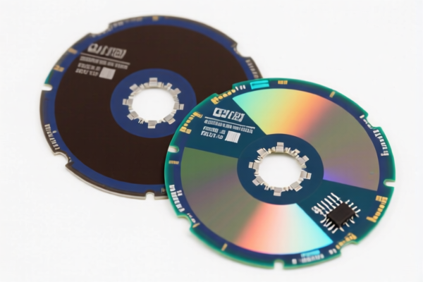
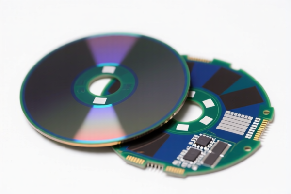
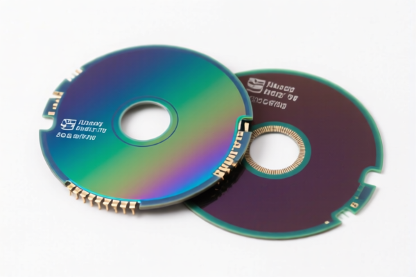
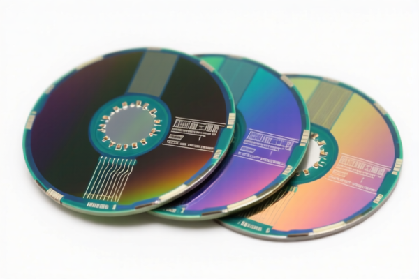
AI Analysis
🧪 Phosphorus-Doped Silicon Wafer (Electronic Grade)
🌐 HS Code Reference & Customs Clearance Guide | 2026 Latest Tariff Analysis | Professional-Grade通关 Strategy
📌 I. Product Definition & Classification: What Exactly Is a "Doped Silicon Wafer"?
A Phosphorus-Doped Silicon Wafer is a foundational component in the semiconductor industry. It consists of a silicon crystal substrate where phosphorus atoms have been introduced (doped) to create an N-type semiconductor material. This process alters the electrical properties of the silicon, making it essential for manufacturing diodes, transistors, and integrated circuits.
In international trade, these wafers are categorized based on their purpose and form:
- Doped for Electronic Use: If the wafer is specifically treated (doped) and shaped for use in electronics, it falls under HS 3818.
- Raw Silicon Material: If it is considered raw material or chemical element form without specific electronic doping treatment for immediate device use, it might be considered under HS 2804 (though less common for finished wafers).
- Semiconductor Devices: If the wafer is further processed into chips/dies, it moves to HS 8541.
⚠️ Key Distinction:
- "Doped for use in electronics" → HS 3818.00.00 (This is the most common classification for processed wafers ready for device fabrication).
- Raw High-Purity Silicon → HS 2804.61.00 (If sold as a chemical element/raw material, not yet doped for specific electronic use).
- Chips/Dies cut from wafers → HS 8541.10.00 (If already processed into individual semiconductor devices).
📦 II. HS Code Classification Details (2026 Latest Tariff Authority Cross-Reference)
Based on the provided DATA, here are the relevant HS Codes for phosphorus-doped silicon wafers:
| HS Code | Product Description | Applicable Scenario | Doping Status |
|---|---|---|---|
| 3818.00.00.20 | Chemical elements doped for use in electronics, in the form of discs, wafers or similar forms; Polycrystalline silicon wafers, doped | Polycrystalline silicon wafers used in electronics | ✅ Doped |
| 3818.00.00.95 | Chemical elements doped for use in electronics, in the form of discs, wafers or similar forms; Other | Monocrystalline silicon wafers (single-crystal) doped for electronics | ✅ Doped |
| 2804.61.00.00 | Hydrogen, rare gases and other nonmetals: Silicon: Containing by weight not less than 99.99 percent of silicon | Undoped ultra-high purity silicon metal/ingots (Raw material) | ❌ Not Doped (Raw) |
| 2804.69.50.00 | Hydrogen, rare gases and other nonmetals: Silicon: Other: Other | Lower purity silicon or other silicon forms | ❌ Not Doped |
| 8541.10.00.40 | Semiconductor devices: Diodes, other than photosensitive or light-emitting diodes (LED): Unmounted chips, dice and wafers | Wafers processed into individual diodes/chips | ✅ Doped + Processed |
| 8541.49.10.10 | Semiconductor devices: Photosensitive/LED: Other diodes: Unmounted chips, dice and wafers | Wafers processed into LED/photovoltaic cells | ✅ Doped + Processed |
🔍 Critical Note:
- Monocrystalline Doped Wafers (most common for ICs) typically fall under 3818.00.00.95 ("Other").
- Polycrystalline Doped Wafers fall under 3818.00.00.20.
- Raw Silicon (99.99% pure, undoped) falls under 2804.61.00.00.
- Do not confuse "doped wafers" with "raw silicon metal." Doping is a specific electronic manufacturing process.
💰 III. 2026 Latest Tariff Rate Details (Including Surtaxes & Policy Additions)
✅ Applicable Country: United States (US)
✅ Country of Origin: China (CN)
✅ Effective Date: From November 10, 2025 (including subsequent imports)
🎯 1. 3818.00.00.95 – Monocrystalline Silicon Wafers, Doped for Electronic Use (Other)
| Item | Content |
|---|---|
| Base Tariff Rate | 0.0% (ad valorem) |
| Section 301 Surtax | +50.0% (Additional duties on Chinese goods) |
| IEEPA Surtax | Included in the 50% (Current rate reflects combined impact) |
| Total Tariff Rate | 50.0% |
| Tax Calculation | CIF Value × 50.0% |
| De Minimis Exemption | ❌ Not Available (deny_de_minimis) |
| Legal Basis Path | USITC:3818.00.00.95 → Section 301/IEEPA Surcharge |
📌 Explanation:
- Phosphorus-doped silicon wafers classified under 3818.00.00.95 are subject to a 50% total tariff.
- The 0% base rate is offset by a 50% surcharge under US trade policies targeting Chinese semiconductor materials.
- This is a high-cost category for importers. Pre-calculation is essential.
🎯 2. 3818.00.00.20 – Polycrystalline Silicon Wafers, Doped
| Item | Content |
|---|---|
| Base Tariff Rate | 0.0% |
| Section 301 Surtax | +50.0% |
| Total Tariff Rate | 50.0% |
| Tax Calculation | CIF Value × 50.0% |
| De Minimis Exemption | ❌ Not Available |
| Legal Basis Path | USITC:3818.00.00.20 → Section 301/IEEPA Surcharge |
📌 Note:
- Same 50% rate as monocrystalline wafers.
- Applies specifically to polycrystalline substrates.
🎯 3. 2804.61.00.00 – Silicon (≥99.99% Pure, Undoped)
| Item | Content |
|---|---|
| Base Tariff Rate | 0.0% |
| Section 301 Surtax | +50.0% |
| Total Tariff Rate | 50.0% |
| Tax Calculation | CIF Value × 50.0% |
| De Minimis Exemption | ❌ Not Available |
| Legal Basis Path | USITC:2804.61.00.00 → Section 301/IEEPA Surcharge |
📌 Warning:
- Even if you claim it is "raw silicon" (HS 2804), if it is imported from China, it still faces 50% total tax.
- Misclassifying doped wafers as raw silicon to avoid duties is illegal and will result in penalties.
🎯 4. 8541.10.00.40 – Unmounted Diodes/Chips (Processed Wafers)
| Item | Content |
|---|---|
| Base Tariff Rate | 0.0% |
| Section 301 Surtax | +50.0% |
| Total Tariff Rate | 50.0% |
| Tax Calculation | CIF Value × 50.0% |
| De Minimis Exemption | ❌ Not Available |
| Legal Basis Path | USITC:8541.10.00.40 → Section 301/IEEPA Surcharge |
📌 Note:
- If the wafer is already cut into chips/dices for diodes, it falls here.
- Still subject to 50% total tariff.
🛠️ IV. Customs Clearance Practical Advice (Battle-Tested Pitfall Guide)
✅ 1. Required Documentation Checklist (None Can Be Omitted)
| Document | Mandatory | Explanation |
|---|---|---|
| ✅ Product Specification Sheet | ✔️ | Must state: Substrate type (Mono/Polycrystalline), Doping element (Phosphorus), Resistivity, Diameter, Thickness. |
| ✅ Doping Certificate | ✔️ | Proof that phosphorus has been introduced. Critical for distinguishing from raw silicon (HS 2804). |
| ✅ Product Photos | ✔️ | Clear images of wafers, labeling, and packaging. |
| ✅ Commercial Invoice | ✔️ | Must clearly state "Phosphorus-Doped Silicon Wafer" and HS Code. |
| ✅ Packing List | ✔️ | Detail weight, dimensions, and number of wafers per box. |
| ✅ Certificate of Origin (CO) | ✔️ | Required to verify Chinese origin (triggers 50% surcharge). |
✅ 2. Declaration Tips (Key Mantra)
🔥 "Doped is 3818, Raw is 2804, Chips are 8541. Wrong Code = 50% Tax + Penalties!"
| Scenario | Correct Declaration | Incorrect Action |
|---|---|---|
| Doped Monocrystalline Wafer | 3818.00.00.95 |
Declare as 2804.61.00.00 → Customs will reclassify & fine |
| Doped Polycrystalline Wafer | 3818.00.00.20 |
Declare as 3818.00.00.95 → Minor error, but still 50% tax |
| Raw Silicon Ingot (Undoped) | 2804.61.00.00 |
Declare as 3818... → Unnecessary complexity, same tax rate |
| Cut Diode Chips | 8541.10.00.40 |
Declare as 3818... → Misclassification of processed device |
✅ 3. Special Case Handling
| Situation | Handling Advice |
|---|---|
| Mixed Shipment | If a shipment contains both raw silicon and doped wafers, declare separately. Do not mix HS Codes. |
| Wafer with Packaging | The packaging (boxes, trays) is included in the CIF value. No separate duty calculation for packaging. |
| Return Repairs | If returning defective wafers, use HS Code 9903.00.00 (temporary import) if eligible, but standard duties may apply if not returned. |
| R&D Samples | If value < $800, still subject to 50% tax (de minimis not allowed for Chinese doped silicon). |
🌍 V. Global Market Comparison (2026 Latest)
| Country/Region | Recommended HS Code | Tariff (China Origin) | Certification | Remarks |
|---|---|---|---|---|
| 🇺🇸 USA | 3818.00.00.95 |
50% | None | High duty. Avoid de minimis. |
| 🇨🇳 China | 3818.00.00.95 |
0% (Import Duty) | None | Low cost. |
| 🇪🇺 EU | 3818.00.00.95 |
0% (Most Favored Nation) | REACH | No surcharge. |
| 🇯🇵 Japan | 3818.00.00.95 |
0% | JIS | No surcharge. |
📌 Conclusion:
- USA is the only major market with 50% surcharge for Chinese-doped silicon wafers.
- EU and Japan offer 0% tariff for standard imports, making them more cost-effective for Chinese exports.
- China itself has 0% import duty for these materials.
📌 VI. Common Errors & Pitfall Guide (Lessons from Blood & Tears)
❌ Mistake 1: Declaring Doped Wafers as "Raw Silicon" (2804.61.00.00)
👉 Consequence: Customs will detect doping levels via lab tests. Reclassification to 3818 + 50% Tax + Penalty!
❌ Mistake 2: Using "Silicon" as a generic description
👉 Consequence: Customs delays for further inspection. Clear description required!
❌ Mistake 3: Assuming De Minimis ($800) applies
👉 Consequence: 50% tax still applies. No exemption for Chinese doped silicon.
❌ Mistake 4: Mixing Mono and Poly wafers under one HS Code
👉 Consequence: Potential misdeclaration. Declare separately (3818.00.00.20 vs 3818.00.00.95).
✅ Correct Practice:
"Phosphorus-Doped Monocrystalline Silicon Wafer, 6-inch, 1-10 Ohm-cm, Electronic Grade, for Semiconductor Manufacturing, Model XYZ"
🎯 VII. Conclusion: Professional Declaration, Save Time, Reduce Costs!
🎯 Remember the Mantra:
🔹 "Doped is 3818, Raw is 2804, Chips are 8541.
🔹 USA 50%, EU/Japan 0%.
🔹 De Minimis is DEAD for this category."
🔹 "HS Code determines life and death. A small error leads to huge penalties!"
📌 Tips:
- If your wafers are originating from Vietnam, Malaysia, or Thailand, you may apply for IEEPA Exemption, reducing the tariff to 0-5%.
- Apply for Advance Ruling with US Customs (CBP) for pre-classification to avoid disputes.
📣 Immediate Action:
📞 Contact a professional customs broker + Provide Product Specs + Apply for HS Code Advance Ruling
🚀 Ensure your phosphorus-doped silicon wafers clear customs smoothly, efficiently, and profitably!
✨ Professional clearance starts with accurate classification!
💼 Every cent of your cost deserves precise calculation!
Customer Reviews
About HS Code Classification
The Harmonized System (HS) is an internationally standardized nomenclature developed by the World Customs Organization (WCO) to classify traded products. Over 200 countries use the HS system as the basis for customs tariffs, trade statistics, and import/export regulations.
Each HS code follows a hierarchical structure:
- Chapter (2 digits) — Broad category of goods (e.g., Chapter 84: Machinery and Mechanical Appliances)
- Heading (4 digits) — More specific grouping within the chapter
- Subheading (6 digits) — Internationally standardized breakdown, used by all WCO member countries
- National subdivisions (8-10 digits) — Country-specific extensions for further classification, such as US HTSUS 10-digit codes
Correct HS code classification is essential for smooth customs clearance, accurate duty payment, and compliance with trade regulations. Misclassification can lead to customs delays, overpayment of duties, or penalties.
When importing from CN to US, the applicable tariff rates may include:
- Most-Favored-Nation (MFN) rate — The standard duty rate applied to WTO members
- General rate — Applied to countries without trade agreements
- Trade remedy duties — Additional tariffs such as Section 301 (anti-dumping), Section 232 (national security), or countervailing duties
The information provided on this page is for reference purposes only. For official classification, please consult with your local customs authority or a licensed customs broker.