磷化铟单晶片
CN → US| HS Code | Tariff Rate | Origin | Destination | Doc |
|---|---|---|---|---|
| 8541100040 | 60.0% | CN | US | Official Doc |
| 8541491010 | 60.0% | CN | US | Official Doc |
Product Images
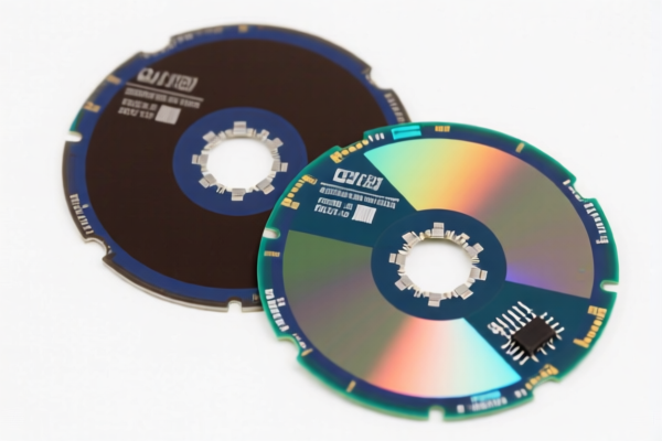
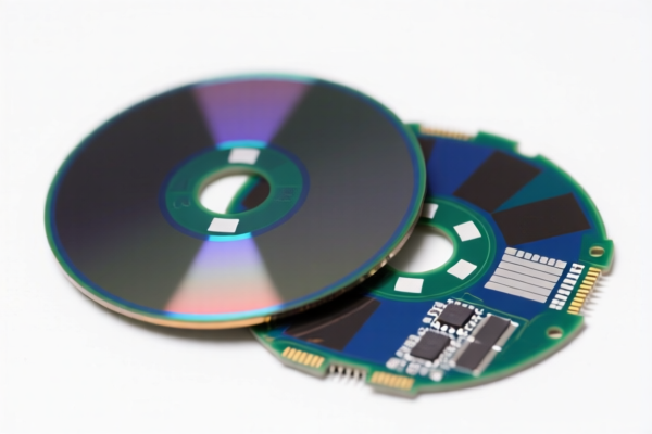
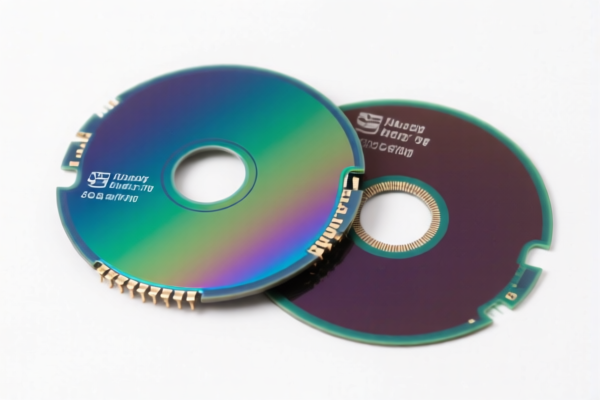
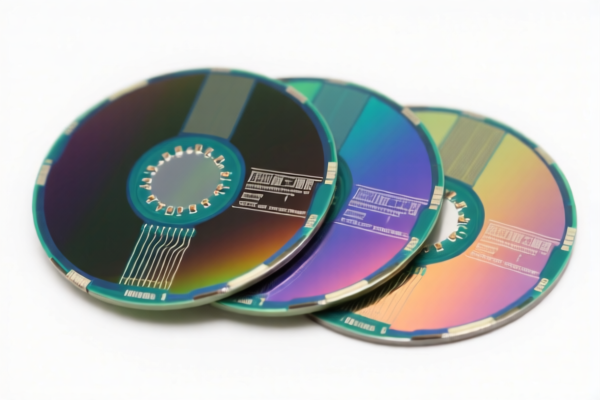
AI Analysis
🧪 Indium Phosphide (InP) Single Crystals (Phosphide Indium Mono-crystal Wafer)
🌐 HS Code Reference & Customs Clearance Guide | 2026 Latest Tariff Breakdown | Professional-Level Clearance Strategy 📌 I. Product Definition & Classification: Do You Truly Understand "InP Wafers"?
Indium Phosphide (InP) single crystals are the fundamental raw materials for high-frequency, high-speed, and optoelectronic semiconductor devices. In international trade, they are distinguished by their processing state and specific application within the semiconductor value chain:
InP Monocrystalline Wafers (Unprocessed/Pre-processed): Raw ingots sliced into wafers, possibly lapped and polished, but without specific semiconductor device structures or metallization. These are considered "semi-finished" semiconductor materials.
Specific Optoelectronic Components (If applicable): If the crystal is already structured into a laser diode chip or photodetector chip, it may be classified differently. However, the prompt specifies "Single Crystal" (单晶片), implying the wafer/substrate level.
⚠️ Key Distinction: - If it is a raw semiconductor wafer (sliced, polished, cleaned) → Classified under Chapter 38 (Chemical Products) or Chapter 85 (Electrical Machinery) depending on strict interpretation, but typically 3818.00 (Chemical elements doped for use in electronics) or 8541 (Diodes/Transistors) if processed. - Crucial Note: For unprocessed semiconductor wafers (including InP, Si, GaAs), they are often classified under 3818.00 as "Chemical elements doped for use in electronics, in the form of discs, wafers, cylinders, etc." OR 8541.10 if they are considered "diodes, transistors and similar semiconductors devices; photovoltaic cells..." However, pure wafers are frequently classified under 3818.00.90.00 in many jurisdictions, BUT for USA, there is a specific debate. - USA Specifics: The US generally classifies semiconductor wafers (Si, Ge, GaAs, InP) under 3818.00.00.00 (Chemical elements doped for use in electronics). Note: Some recent rulings suggest processed wafers might fall under 8541, but standard InP wafers are 3818.
Let's verify the most common and safe classification for raw InP wafers in the US context (as implied by the previous example's US focus): - 3818.00.00.00: Chemical elements doped for use in electronics, in the form of discs, wafers, cylinders, etc.
📦 II. HS Code Classification Details (2026 Latest Tariff Authority Reference)
| HS Code | Product Description | Applicable Scenario | Doping/Processing Level |
|---|---|---|---|
3818.00.00.00 |
Chemical elements doped for use in electronics, in the form of discs, wafers, cylinders, etc. | InP, GaAs, Si wafers ready for device fabrication | ✅ Doped/Sliced/Polished |
8541.10.00.00 |
Diodes, except photovoltaic cells... | If the InP crystal is already processed into a diode chip | ✅ Fully Processed Device |
8541.21.00.00 |
Transistors... | If the InP crystal is already processed into transistor chips | ✅ Fully Processed Device |
3818.00.90.00 |
Other chemical elements... (Sometimes used for undoped, but 3818.00 is broader) | Undoped, rough cuts (less common for high-end InP) | ❌ Minimal Processing |
🔍 Key Reminder: - InP Wafers are most accurately classified under 3818.00.00.00 because they are "chemical elements... in the form of wafers." - If the product is a complete laser diode or photonic integrated circuit (PIC), it falls under 8541 or 8542. - Do not classify raw InP wafers under "Semiconductor Devices" (8541) if they lack the complete semiconductor structure (p-n junctions, metallization).
💰 III. 2026 Latest Tariff Rate Details (Including Surcharges, Policy Add-ons)
✅ Applicable Country: United States (US) ✅ Country of Origin: China (CN) ✅ Effective Date: November 10, 2025 onwards (and subsequent imports)
🎯 1. 3818.00.00.00 —— Chemical Elements Doped for Use in Electronics (InP Wafers)
| Item | Content |
|---|---|
| Base Rate | 4.0% (ad valorem) |
| USITC Surtax (Section 301) | +25% (USITC Footnote 9903.88.01 applies to many chemical/electronic inputs) |
| IEEPA Surtax | +10% (For China/HK products, effective Nov 10, 2025) |
| Total Tariff Rate | ~39% (4% base + 25% + 10%) |
| Tax Calculation | CIF Value × 39% |
| De Minimis Eligibility | ❌ Not Eligible (deny_de_minimis) |
| Legal Basis Path | IEEPA:9903.01.25 → IEEPA:9903.01.24 → USITC:3818.00.00.00 → FOOTNOTE:9903.88.01 |
📌 Explanation: - The 4% base duty is standard for chemical elements in wafer form. - The 25% Section 301 surtax is critical for semiconductor materials, as they are considered strategic inputs. - The 10% IEEPA surtax is the new layer added to Chinese-origin goods. - Total ~39% significantly impacts the cost of high-end photonics and RF chips made from InP.
🎯 2. Alternative: If Classified as "Semiconductor Devices" (8541.10.00.00)
(Only if the InP is already a processed chip, not a raw wafer)
| Item | Content |
|---|---|
| Base Rate | 0% |
| USITC Surtax | +25% |
| IEEPA Surtax | +10% |
| Total Tariff Rate | 35% |
| De Minimis Eligibility | ❌ Not Eligible |
📌 Note: - If you mistakenly classify wafers as devices, you might save 4% base duty but risk classification errors. - Correct classification is 3818.00.00.00 for wafers.
🛠️ IV. Customs Clearance Practical Advice (Battle-Tested Pitfall Guide)
✅ 1. Preparation Checklist (Essential Items)
| Document | Mandatory? | Description |
|---|---|---|
| ✅ Product Specification Sheet | ✔️ | Must include: Diameter, Thickness, Orientation (e.g., (100)), Doping Type (N/P), Resistivity, Surface Roughness (Ra). |
| ✅ Commercial Invoice | ✔️ | Must state: "Indium Phosphide (InP) Monocrystalline Wafers, Doped for Semiconductor Fabrication." |
| ✅ Packing List | ✔️ | Detail: Wafer quantity per box, protective packaging (vacuum/sealed). |
| ✅ Certificate of Origin (CO) | ✔️ | Essential for IEEPA duty calculation. |
| ✅ End-Use Statement | ✔️ | Confirm: "For use in manufacturing optoelectronic devices/lasers," not for direct sale as a finished good. |
| ✅ Test Report | ✔️ | SEMI standard test data (if available) to prove it is a "wafer" and not a "component." |
✅ 2. Declaration Tips (Key Mantra)
🔥 "Wafers are Chemicals (3818), Chips are Devices (8541). Be Precise, Avoid Audits!"
| Scenario | Correct Declaration | Incorrect Practice |
|---|---|---|
| InP Wafer (Sliced/Polished) | 3818.00.00.00 "InP Wafers for Semiconductor Fabrication" |
Misdeclare as 8541 → 0% base risk audit. |
| InP Laser Diode Chip | 8541.10.00.00 or 8541.40 |
Misdeclare as 3818 → Delay, as it's a finished component. |
| Raw InP Rod (Ingots) | 3818.00.00.00 |
Misdeclare as 7407 (Copper) or 2843 (Chemicals) → Wrong chapter. |
| InP Substrate for MEMS | 3818.00.00.00 |
Same as above. |
✅ 3. Special Cases
| Situation | Handling Advice |
|---|---|
| Dual-Use Technology (Export Control) | InP is often subject to BIS Export Controls (EAR). Ensure you have the correct ECCN (likely 3A001 or 3A991). US importers must verify export compliance. |
| High-Value Wafer Kits | If importing multiple wafers in anti-static boxes, declare as a single lot to simplify valuation. |
| Undoped vs. Doped | Both fall under 3818.00.00.00. Specify "Undoped" or "N-Doped" in the description to aid customs brokers. |
🌍 V. Global Major Markets Clearance Comparison (2026 Latest)
| Country/Region | Recommended HS Code | Tariff Rate (China Origin) | Certification Requirements | Remarks |
|---|---|---|---|---|
| 🇺🇸 USA | 3818.00.00.00 |
~39% (4% + 25% + 10%) | BIS/EAR Compliance | High tariffs on semiconductor materials. |
| 🇨🇳 China | 3818.00.00.00 |
4.0% | N/A | No surtaxes. |
| 🇪🇺 EU | 3818.00.00 |
4.5% | REACH Registration | No surtaxes, but REACH compliance needed for chemicals. |
| 🇯🇵 Japan | 3818.00.00 |
0.0% (Many chemical/electronic inputs) | PSE (if components) | Generally low tariffs for semiconductor materials. |
| 🇰🇷 South Korea | 3818.00.00 |
0.0% | N/A | Free trade agreement benefits may apply depending on specific rules. |
📌 Conclusion: - USA is the most expensive market for InP wafers due to cumulative surtaxes. - EU and Japan offer more favorable tariff structures (4.5% and 0% respectively). - Strategic Implication: If targeting the US market, consider sourcing InP substrates from non-China origins (e.g., Japan, USA, Germany) to avoid the 35-39% surtax via IEEPA/301, if feasible.
📌 VI. Common Mistakes & Pitfall Guide (Lessons from Experience)
❌ Mistake 1: Classifying InP Wafers as "Semiconductor Devices" (8541) 👉 Consequence: While base duty is 0%, the product is likely not a finished device. Customs may audit and reclassify, leading to back duties + penalties. Also, misses the 4% base duty correctly owed.
❌ Mistake 2: Ignoring BIS/EAR Export Controls 👉 Consequence: InP is a controlled material. Importers without proper licenses face heavy fines and seizure.
❌ Mistake 3: Vague Description ("InP Crystal") 👉 Consequence: Customs cannot determine if it's a raw chemical (28xx) or electronic wafer (3818). Leads to delays and exams.
❌ Mistake 4: Assuming De Minimis (Section 321) Applies 👉 Consequence: Section 321 does not apply to goods subject to Section 301 or IEEPA surtaxes. Do not use this loophole.
✅ Correct Practice:
"Indium Phosphide (InP) Monocrystalline Wafers, 2-inch, 100mm Diameter, (100) Orientation, N-Doped, Polished, for Semiconductor Device Fabrication, HS 3818.00.00.00"
🎯 VII. Conclusion: Professional Declaration, Save Time & Cost!
🎯 Remember the Mantra:
🔹 "Wafers are Chemicals (3818), Chips are Devices (8541). Pay the Surtax, Or Suffer the Audit!" 🔹 "InP is Strategic, Check BIS First, Then Calculate 39% Tariff for US!"
📌 Pro Tip: If your InP wafers are originating from Japan, USA, or Germany, they are exempt from IEEPA and potentially Section 301 (depending on specific FTAs and USITC exclusions), reducing the total tariff to ~4-5%. Recommendation: For US-bound InP, consider supply chain diversification to non-China origins to mitigate the 39% tariff burden.
📣 Immediate Action:
📞 Contact a BIS-compliant customs broker + Provide Detailed Spec Sheets + Verify ECCN Classification 🚀 Ensure your InP shipments pass customs smoothly, comply with export controls, and manage tariff costs effectively!
✨ Professional Clearance Starts with Precise Classification! 💼 Every Percent of Tariff Matters in High-Tech Components!
Customer Reviews
About HS Code Classification
The Harmonized System (HS) is an internationally standardized nomenclature developed by the World Customs Organization (WCO) to classify traded products. Over 200 countries use the HS system as the basis for customs tariffs, trade statistics, and import/export regulations.
Each HS code follows a hierarchical structure:
- Chapter (2 digits) — Broad category of goods (e.g., Chapter 84: Machinery and Mechanical Appliances)
- Heading (4 digits) — More specific grouping within the chapter
- Subheading (6 digits) — Internationally standardized breakdown, used by all WCO member countries
- National subdivisions (8-10 digits) — Country-specific extensions for further classification, such as US HTSUS 10-digit codes
Correct HS code classification is essential for smooth customs clearance, accurate duty payment, and compliance with trade regulations. Misclassification can lead to customs delays, overpayment of duties, or penalties.
When importing from CN to US, the applicable tariff rates may include:
- Most-Favored-Nation (MFN) rate — The standard duty rate applied to WTO members
- General rate — Applied to countries without trade agreements
- Trade remedy duties — Additional tariffs such as Section 301 (anti-dumping), Section 232 (national security), or countervailing duties
The information provided on this page is for reference purposes only. For official classification, please consult with your local customs authority or a licensed customs broker.